AD9446
PRODUCTION16-Bit, 80 MSPS / 100 MSPS A/D Converter
- Part Models
- 2
- 1ku List Price
- Starting From $74.39
Overview
- 100 MSPS guaranteed sampling rate (AD9446-100)
- 83.6 dBFS SNR with 30 MHz input (3.8 V p-p input, 80 MSPS)
- 82.6 dBFS SNR with 30 MHz input (3.2 V p-p input, 80 MSPS)
- 89 dBc SFDR with 30 MHz input (3.2 V p-p input, 80 MSPS)
- 95 dBFS 2-tone SFDR with 9.8 MHz and 10.8 MHz (100 MSPS)
- 60 fsec rms jitter
- Excellent linearity
DNL = ±0.4 LSB typical
INL = ±3.0 LSB typical
- 2.0 V p-p to 4.0 V p-p differential full-scale input
- Buffered analog inputs
- LVDS outputs (ANSI-644 compatible) or CMOS outputs
- Data format select (offset binary or twos complement)
- Output clock available
- 3.3 V and 5 V supply operation
The AD9446 is a 16-bit, monolithic, sampling analog-to-digital converter (ADC) with an on-chip track-and-hold circuit. It is optimized for performance, small size, and ease of use. The product operates up to 100 MSPS, providing superior SNR for instrumentation, medical imaging, and radar receivers employing baseband (<100 MHz) IF frequencies.
The ADC requires 3.3 V and 5.0 V power supplies and a low voltage differential input clock for full performance operation. No external reference or driver components are required for many applications. Data outputs are LVDS-compatible (ANSI-644) or CMOS-compatible and include the means to reduce the overall current needed for short trace distances.
Optional features allow users to implement various selectable operating conditions, including data format select and output data mode.
The AD9446 is available in a 100-lead surface-mount plastic package (100-lead TQFP/EP) specified over the industrial temperature range (−40°C to +85°C).
PRODUCT HIGHLIGHTS
- True 16 bit linearity.
- High performance: outstanding SNR performance for baseband IFs in data acquisition, instrumentation, magnetic resonance imaging, and radar receivers.
- Ease of use: On-chip reference and high input impedance track-and-hold. An output clock simplifies data capture.
- Packaged in a Pb-free, 100-lead TQFP/EP.
- Clock duty cycle stabilizer (DCS) maintains overall ADC performance over a wide range of clock pulse widths.
- OR (out-of-range) outputs indicate when the signal is beyond the selected input range.
APPLICATIONS
- MRI receivers
- Multi-carrier, multimode cellular receivers
- Antenna array positioning
- Power amplifier linearization
- Broadband wireless
- Radar, infrared imaging
- Communications instrumentation
Documentation
Data Sheet 1
Application Note 13
Technical Articles 1
Analog Dialogue 4
ADI has always placed the highest emphasis on delivering products that meet the maximum levels of quality and reliability. We achieve this by incorporating quality and reliability checks in every scope of product and process design, and in the manufacturing process as well. "Zero defects" for shipped products is always our goal. View our quality and reliability program and certifications for more information.
| Part Model | Pin/Package Drawing | Documentation | CAD Symbols, Footprints, and 3D Models |
|---|---|---|---|
| AD9446BSVZ-100 | 100-Lead TQFP (14mm x 14mm) | ||
| AD9446BSVZ-80 | 100-Lead TQFP (14mm x 14mm) |
| Part Models | Product Lifecycle | PCN |
|---|---|---|
|
Mar 15, 2016 - 14_0258 Assembly Transfer of Selected 14x14 LQFP, 14x14 LQFP_EP and 7x7,10x10,12x12,14x14 TQFP_EP Products to Amkor Philippines |
||
| AD9446BSVZ-100 | ||
| AD9446BSVZ-80 | ||
|
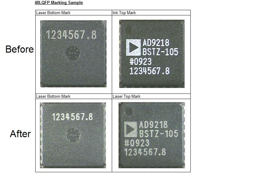
Jun 16, 2009 - 09_0027 Conversion to Laser Mark for the LQFP Packages (Single Grades) |
||
| AD9446BSVZ-100 | ||
| AD9446BSVZ-80 | ||
This is the most up-to-date revision of the Data Sheet.
Software Resources
Can't find the software or driver you need?
Request a Driver/SoftwareHardware Ecosystem
| Parts | Product Life Cycle | Description |
|---|---|---|
| Clock ICs 6 | ||
| AD9510 | RECOMMENDED FOR NEW DESIGNS | 1.2 GHz Clock Distribution IC, PLL Core, Dividers, Delay Adjust, Eight Outputs |
| AD9511 | RECOMMENDED FOR NEW DESIGNS | 1.2 GHz Clock Distribution IC, PLL Core, Dividers, Delay Adjust, Five Outputs |
| AD9512 | RECOMMENDED FOR NEW DESIGNS | 1.2 GHz Clock Distribution IC, Two 1.6 GHz Inputs, Dividers, Delay Adjust, Five Outputs |
| AD9513 | RECOMMENDED FOR NEW DESIGNS | 800 MHz Clock Distribution IC, Dividers, Delay Adjust, Three Outputs |
| AD9514 | RECOMMENDED FOR NEW DESIGNS | 1.6 GHz Clock Distribution IC, Dividers, Delay Adjust, Three Outputs |
| AD9515 | RECOMMENDED FOR NEW DESIGNS | 1.6 GHz Clock Distribution IC, Dividers, Delay Adjust, Two Outputs |
| Differential Amplifiers 2 | ||
| ADA4938-1 | RECOMMENDED FOR NEW DESIGNS | Ultralow Distortion Differential ADC Driver (Single) |
| AD8352 | RECOMMENDED FOR NEW DESIGNS | 2 GHz Ultralow Distortion Differential RF/IF Amplifier |
| RF Amplifiers 2 | ||
| ADA4932-1 | RECOMMENDED FOR NEW DESIGNS | Low Power Differential ADC Driver |
| AD8375 | PRODUCTION | Ultralow Distortion IF VGA |
Tools & Simulations
Virtual Eval - BETA
Virtual Eval is a web application to assist designers in product evaluation of ADCs, DACs, and other ADI products. Using detailed models on Analog’s servers, Virtual Eval simulates crucial part performance characteristics within seconds. Configure operating conditions such as input tones and external jitter, as well as device features like gain or digital down-conversion. Performance characteristics include noise, distortion, and resolution, FFTs, timing diagrams, response plots, and more.
Open ToolVisual Analog
For designers who are selecting or evaluating high speed ADCs, VisualAnalog™ is a software package that combines a powerful set of simulation and data analysis tools with a user-friendly graphical interface.
Open ToolADIsimRF
ADIsimRF is an easy-to-use RF signal chain calculator. Cascaded gain, noise, distortion and power consumption can be calculated, plotted and exported for signal chains with up to 50 stages. ADIsimRF also includes an extensive data base of device models for ADI’s RF and mixed signal components.
Open ToolAD9446 Simulink ADIsimADC Model
Open ToolAD9446 IBIS Models 1
Evaluation Kits
AD9446 Evaluation Board