AD4060
推荐用于新设计紧凑型、低功耗、12 位、易驱动 SAR ADC,带 I3C 接口
- 产品模型
- 3
概述
- 尺寸小,性能强大
- INL:0.1 LSB(最大值)
- SNR:73.8dB,VREF = 3.3V
- 每次转换 1.35nJ
- 采样模式下 300kSPS 时为 405μW
- 自主模式下 1MSPS/300kSPS 时为 370μW/112μW
- 4.1μW 待机功耗
- 多功能信号调理集成
- Easy Drive 功能可实现小型、低功耗 AFE 设计
- 兼容差分和单端信号链
- 宽共模输入范围
- 最大限度地减少数字设备活动和功耗
- 使用窗口比较器和中断生成的自主采样
- 支持突发采样的平均滤波器
- 配套设备的电源循环同步化
- 2 线 I3C 接口兼容 1.8V 至 3.3V 逻辑
- 2.00mm × 2.6mm LFCSP 和 1.67mm × 1.97mm WLCSP
- 宽工作温度范围:−40°C 至 +125°C
AD4060 是一款多功能 12 位逐次逼近寄存器 (SAR) 模数转换器 (ADC),可实现低功耗、高密度数据采集解决方案,且不会牺牲精度。该 ADC 在性能和高功效比之间实现了独特的平衡,并具有创新功能,可根据系统的当前需求在高分辨率和低功耗模式之间无缝切换。AD4060 非常适合电池供电、紧凑型数据采集和终端感应应用。
Easy Drive 功能可实现高效的模拟前端(AFE)设计。小型采样电容器(3.4pF)可最大限度地提高输入阻抗,从而减少对 SAR ADC 通常需要的高带宽、耗电放大器的依赖。宽输入共模范围为差分和单端信号提供了固有支持。
AD4060 支持具有关断模式和中断驱动固件的微控制器。自主模式可以在数字主机休眠时检测超出范围的事件。突发平均模式可提供按需的高分辨率测量,同时卸载主机处理器的计算。自定时设备使能信号(DEV_EN)将 AFE 套件电源循环与 ADC 采样时刻同步,从而优化系统功耗,同时最大限度地减少上电稳定误差伪影。AD4060 还支持对基准电压源进行电源循环,并使用该电源作为 ADC 基准电压源(VREF),以节省更多电量。
设备配置和 ADC 数据读回通过强大的双线 I3C 接口支持,并且所有数据传输均支持循环冗余校验 (CRC)。AD4060 采用紧凑型 14 引线框架芯片规模 [LFCSP] 和 16 球晶圆级芯片规模 [WLCSP] 封装,可在很宽的温度范围内工作,非常适合各种应用。
应用
- 电池供电的数据采集
- 生命体征监测
- 生物和化学分析
- 地质和地震监测
- 运动与机器人
参考资料
数据手册 1
用户手册 1
设计笔记 1
ADI 始终高度重视提供符合最高质量和可靠性水平的产品。我们通过将质量和可靠性检查纳入产品和工艺设计的各个范围以及制造过程来实现这一目标。出货产品的“零缺陷”始终是我们的目标。查看我们的质量和可靠性计划和认证以了解更多信息。
| 产品型号 | 引脚/封装图-中文版 | 文档 | CAD 符号,脚注和 3D模型 |
|---|---|---|---|
| AD4060BCBZ-RL7 | WLCSP | ||
| AD4060BCPZ-R2 | LFCSP | ||
| AD4060BCPZ-RL7 | LFCSP |
软件资源
Evaluation Software 1
找不到您所需的软件或驱动?
硬件生态系统
工具及仿真模型
LTspice
LTspice中提供以下器件型号:
- AD4060
信号链设计器
信号链设计器是一款网页端工具,可创建和仿真复杂的精密信号链。确定PCB设计之前,先检查电路性能:传递函数、噪声、功耗、输入范围和直流误差。快速尝试不同的器件和架构。可将信号链导出到LTspice以便进一步分析。
打开工具
LTspice®是一款强大高效的免费仿真软件、原理图采集和波形观测器,为改善模拟电路的仿真提供增强功能和模型。
评估套件
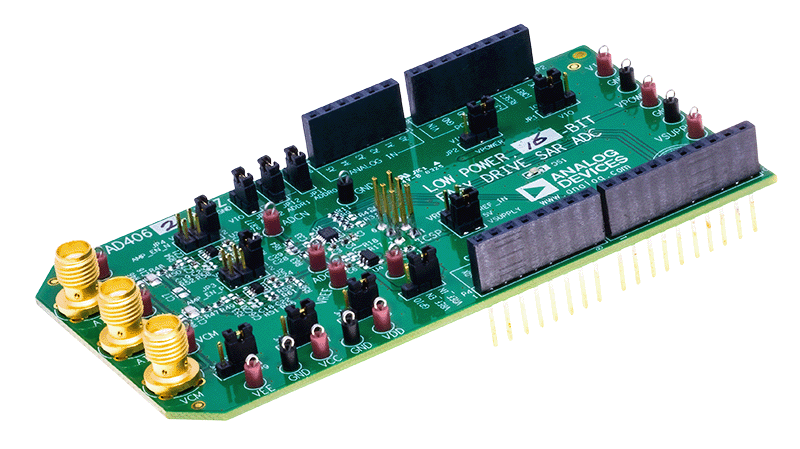
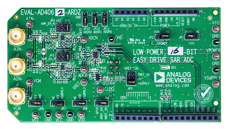
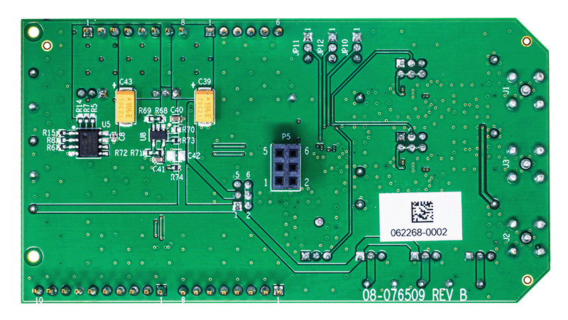
EVAL-AD4062
Evaluating the AD4060/AD4062 Compact, Low Power, 12-Bit/16-Bit, 2MSPS Easy Drive SAR ADCs
资料
最新评论
需要发起讨论吗? 没有关于 AD4060的相关讨论?是否需要发起讨论?
在EngineerZone®上发起讨论