Battery-Free Power Backup System Uses Supercapacitors to Prevent Data Loss in RAID Systems
Battery-Free Power Backup System Uses Supercapacitors to Prevent Data Loss in RAID Systems
著者
Jim Drew
2010年10月01日
RAID systems by their very nature are designed to preserve data in the face of adverse circumstances. One such circumstance, a power failure, does not directly threaten data that is stored on disks, but it does compromise data in transit or data that is temporarily stored in volatile memory. To protect volatile data, many systems incorporate a battery-based power backup system that supplies short-term power—enough watt-seconds for the RAID controller to write volatile data to nonvolatile memory.
The problem is that increased performance demands and green initiatives are putting pressure on system designers to find alternatives to batteries. Batteries are a notoriously hazardous material that must be disposed of under the strict guidelines set by regulatory agencies. Because they require regular replacement whether used or not, battery replacement and disposal is a serious consideration in the cost of running a data center.
Advancements in flash memory performance have made it possible to replace the batteries in these systems with longer-lasting, higher performance and greener supercapacitors. Supercapacitors are made of carbon and aluminum and contain no heavy metals, so they do not present any hazardous material disposal issues. Also, supercapacitors are more robust than batteries, thus decreasing maintenance costs—the cycle life of Li-ion batteries is 500 cycles while a supercapacitor offers a cycle life of one million cycles. Supercapacitors can be recharged to full capacity in minutes where as batteries may take as long as six hours. Although the energy density of a supercapacitor may be as much as two orders of magnitude less than a Li-ion battery, reduced power requirements in flash memory and increased supercapacitor capacities have made them a viable energy storage medium for data-recovery backup solutions.
In a supercapacitor-based backup power system, a series connected capacitor stack must be charged and the cell voltages balanced. The supercapacitors are witched into the power path when needed and the power to the load is controlled by a DC/DC converter. Figure 1 shows a supercapacitor-based power backup system using an LTC3625 supercapacitor charger, an automatic power crossover switch using the LTC4412 and an LTM4616 dual output DC/DC converter.

Figure 1. Circuit implementation of a supercapacitor energy storage system for holding up power during a power fault.
The LTC3625 is a high efficiency supercapacitor charger that has a number of features that makes it an ideal choice for small profile backup in RAID applications. It comes in a 3mm × 4mm × 0.75mm 12-lead DFN package and requires few external parts. It features programmable average charge current up to 1A, automatic voltage cell balancing of two series-connected supercapacitors and a low quiescent current. When the input power is removed or the part is disabled, the LTC3625 automatically enters a low current state drawing less than 1µA from the supercapacitors.
Supercapacitor Characteristics
Supercapacitors are available in capacitances that range from the hundreds of millifarads to thousands of farads. The standard voltage ratings are 2.5V and 2.7V, while packaged, stacked supercapacitors can be greater than 15V. A 10F/2.7V supercapacitor is available in a 10mm × 30mm 2-terminal radial can while a 400F/2.7V supercapacitor is in a 35mm × 62mm 4-terminal radial can. Two of the four terminals in the larger can are for mechanical stability and are not electrically connected to either power terminal.
The two critical parameters of the supercapacitor to a backup power application are the initial leakage current and the cell voltage. The initial leakage current may be as much as 50 times the rated leakage current and decreases to the specified current after 100 hours at rated voltage. The applied voltage across the supercapacitor has a significant effect on its operating life. When charging series connected supercapacitors, voltage balancing is a key requirement of the charging circuit to preserve capacitor life. Passive voltage balancing, where a resistor is placed in parallel with each supercapacitor, is a simple technique but one that continually discharges the supercapacitor when the charger is disabled. Active voltage balancing, such as that performed by the LTC3625 during the charging process, eliminates the need for these resistors and prevents overcharging of the supercapacitors.
Backup Power Applications
An effective power backup system incorporates a supercapacitor stack that has the capacity to support a complete data transfer out of volatile memory. A DC/DC converter takes the output of the supercapacitor stack and provides a constant voltage to the data recovery electronics. The data transfer must be completed before the voltage across the supercapacitor stack drops to the minimum input operating voltage (VUV) of the DC/DC converter.
To estimate the minimum capacitance of the supercapacitor stack, the effective circuit resistance (RT) needs to be determined. RT is the sum of the ESR of the supercapacitors, the distribution losses (RDIST) and the RDS(ON) of the automatic crossover’s MOSFETs.
![]()
Allowing 10% of the input power to be lost in the effective circuit resistance at the point when the voltage into the DC/DC converter is at VUV, the maximum value of RT may be determined by:

The voltage required across the supercapacitor stack (VC(UV)) at this minimum operating voltage of the DC/DC converter:

The minimum capacitance (CMIN) requirement can now be calculated based on the required backup time (TBU) to transfer data into the flash memory, the initial stack voltage (VC(0)) and (VC(UV)).

The minimum capacitance (CMIN) is the effective capacitance (CEFF) of the stack of supercapacitors, which is the capacitance of one supercapacitor divided by the number of supercapacitors in the stack. The ESR used in the expression for calculating RT is the product of the ESR of one supercapacitor times the number of supercapacitors in the stack. The end of life of a supercapacitor is defined as when the capacitance drops to 70% of its initial value or the ESR doubles in value. This end of life definition is used in selecting the supercapacitor for the design.
Both the ESR and capacitance of the supercapacitor decrease as the applied frequency increases. Manufactures generally specify the ESR at 1kHz while some specify the ESR at 1kHz as well as at DC. The capacitance is usually specified at DC. One method of determining the actual capacitance and ESR of the supercapacitor is to apply a constant current (I) to a charged supercapacitor and use the voltage decay to determine these parameters. The initial step in voltage (∆VC), neglecting any inductance effect of the supercapacitor, is used to determine the ESR.

After the initial step in voltage, the voltage across the supercapacitor decreases linearly due to the constant current load. By measuring the voltage at two time intervals, the capacitance of the supercapacitor can be determined.
VC(t1) is the voltage at the first time interval (t1)
VC(t2) is the voltage at the second time interval (t2)

The final parameter to determine is the charging current (ICHARGE) of the supercapacitors. The charging current is determined by the desired recovery time or recharge time (TRECHARGE) of the stack of supercapacitors.
The charging profile of the supercapacitors using the LT3625 is not the classic linear voltage ramp that one would expect (see Figure 2). This is due to the buck-boost topology of the LT3625.

Figure 2. Charge profile into matched supercaps
The bottom supercapacitor of a two-capacitor stack is charged first to approximately 1.35V (VMID(GOOD)). Once the bottom capacitor reaches 1.35V the boost circuit starts to charge the top supercapacitor, emoving charge from the bottom supercapacitor. The buck converter continues to charge the bottom supercapacitor but the rise in voltage is slower since some of its charge is being removed. If the boost converter’s input current is greater than the buck converters output current, voltage on the bottom supercapacitor decreases, and when it decays by the VMID(GOOD) hysteresis, the boost converter turns off and remains off until the bottom supercapacitor charges back to VMID(GOOD).
If the top supercapacitor exceeds the bottom supercapacitor by 50mV, the boost converter turns off until the bottom supercapacitor is 50mV above the top supercapacitor. Finally if the bottom supercapacitor reaches its maximum threshold, the buck converter turns off and the boost converter remains on. The voltage on the bottom supercapacitor deceases and the buck converter remains off until the voltage decreases by 50mV. This process continues until VOUT reaches its programmed charger termination voltage.
The graph in Figure 2 shows the charge profile for two configurations of the LTC3625 charging a stack of two 10F supercapacitors to 5.3V with RPROG set to 143k. This graph, combined with the following equation, is used to determine the value of RPROG that would produce the desired charge time for the actual supercapacitors in the target application.

VC(UV) is the minimum voltage of the supercapacitors at which the DC/DC converter can produce the required output. VOUT is the output voltage of the LTC3625 in the target application (set by VSEL pin). TESTIMATE is the time required to charge from VC(UV) to the 5.3V, as extrapolated from the charge profile curves. TRECHARGE is the desired the recharge time in the target application.
The initial charge time at startup is determined from the full charging time of 70 seconds.

Design Example
For example, say it takes 45 seconds to store the data into flash memory where the input power to the DC/DC converter is 20W. VUV of the DC/DC converter is 2.7V. A TRECHARGE of ten minutes is desired. The voltage applied to the supercapacitor directly affects its lifetime so we do not want to apply full rated voltage (2.7V) across each stacked cap. The full charge voltage of the stack is set to 4.8V—a good compromise between extending the life of the supercapacitor and utilizing as much of the storage capacity as possible. The components of RT are estimated: RDISTRIBUTION = 10mΩ, ESR = 20mΩ and RDS(ON) = 10mΩ.

The resulting estimated values of RT(MAX) = 36mΩ and RT = 40mΩ are close enough for this stage of the design. The voltage needed on the supercapacitor stack when the DC/DC converter drops out is:

The require capacitance of the stack is:

A stack of two 360F supercapacitors (NessCap ESHSR-0360C0-002R7A) have an end-of-life capacitance of 126F. The initial ESR is specified at 3.2mΩ with an end of life ESR at 6.4mΩ.
The crossover switch consists of an LTC4412 PowerPath™ controller and two Si4421DY, P-Channel MOSFETs from Vishay. The RDS(ON) of the Si4421DY with a gate voltage of 2.5V is 10.75mΩ (max).
Using the values for the end of life ESR of the supercapacitors and the actual MOSFET’s RDS(ON), the maximum interconnect resistance can be determined:

The LTC3625 has two configuration modes of operation. A single inductor configuration is used for supercapacitor charging currents of less than 0.5A and a dual inductor configuration for charging currents up to 1A. For this application, the 2-inductor configuration is used to meet the recharging time requirement with the 360F supercapacitors.
To determine the value for RPROG, the stack capacitance is estimated at the supercapacitors initial capacitance plus the high side (20%) of its tolerance. From the graph in Figure 2, the charge time from 3V to 5.3V was estimated at 32 seconds.

The nearest standard 1% resistor is 78.7k.
The initial start-up time is estimated at:

The data sheet suggests a 3.3µH inductor (Coilcraft MSS7341-332NL) for both the buck and boost inductors.
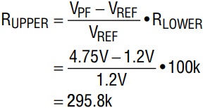
The LTC3625 contains a power fail comparator, which is used to monitor the input power to enable the LTC4412 PowerPath controller. The PFO comparator has an internal reference of 1.2V connected to the comparator’s negative input. A voltage divider connected to the PFI pin sets the power fail trigger point (VPF) to 4.75V. The bottom resistor is set to 100k, so the upper resistor is:

The nearest standard 1% resistor is 294k.
The Circuit in Action
Figure 1 shows a complete supercapacitor energy storage system consisting of the LT33625, two Coilcraft 3.3µH inductors and two 360F supercapacitors from NessCap. The LTC4412 and the two Vishay Si4421DY MOSFETs make up the automatic crossover switch while the LTM4616 is the DC/DC converter that represents the constant power load to the energy storage system.
Figure 3 shows an initial charging time of 1112 seconds for the LTC3625 charging circuit. Using nominal component values the initial charging time is 1255 seconds, which is well within component tolerance levels. During the first 250 seconds, only the buck converter is charging the bottom supercapacitor and once the voltage reaches 1.35V, the boost converter starts to operate. Both the buck converter and the boost converter continue to operate for the next 500 seconds. An interesting observation of the charging profile is that after 750 seconds, the change in slope and the ripple voltage on the input voltage is due to the buck converter turning off and on during the final minutes of charging.

Figure 3. Initial charging of a depleted series connected pair of 360F supercapacitors
Figure 4 shows the backup time of the system with a 20W load. The desired backup time was 45 seconds while our system is supporting the load for 76.6 seconds. The longer available backup time is due to lower than estimated parasitic circuit resistances and that the DC/DC converters continue to operate down to 2.44V instead of the 2.7V in the design calculations. The output of the 1.8V converter can be seen to turn back on again when the 1.2V converter turns off. This “motor-boating” effect is caused by the rise in voltage at the input of the DC/DC converter when the input current is reduce as the 1.2V converter section turns off. This can be eliminated by adding an external undervoltage lockout circuit with adequate hysteresis to disable the DC/DC converter.

Figure 4. Supercapacitor backup time supporting a 20W Load
Finally, Figure 5 shows the recharge time of the supercapacitors after a backup operation. The recharge time is actually 685 seconds, compared to the 600 seconds used in the calculations. The longer charging time is attributed to the lower starting voltage of 2.44V for the DC/DC converter.

Figure 5. Recharge of series-connected pair of 360F supercapacitors
Conclusion
Supercapacitors are replacing batteries to satisfy green initiative mandates for data centers. The LTC3625 is an efficient 1A supercapacitor charger with automatic cell balancing that can be combined with the LTC4412 low loss PowerPath controller to produce an energy storage system that protects data in RAID disk applications. The LTC3625 is available in a 12-lead 3mm × 4mm × 0.75mm DFN package.
著者について
Jim Drew。2007年アナログ・デバイセズに入社。同社ボストン(マサチューセッツ州)の設計センターでシニア・アプリケーション・エンジニアとして勤務。アプリケーション固有パワーICのアプリケーション・サポートを担当ソーラー電力、エナジー・ハーベスティング、スーパーキャパシタ・チャージャ・アクティブ・バッテリ・バランシングなどを対象とするパワー・コンディショニング・アプリケーションに関心を持つ。これまで、EMC、Hewlett Packa...


