概要
本稿で取り上げるのは、ソフトウェア無線(SDR:Software-defined Radio)の機能を実現するSOM(System-on-Module)です。そのSOMは、集積度の高いCOTS(Commercial Off-The-Shelf)の製品として提供されています。想定される用途は、電子戦(EW:Electronic Warfare)向けのモバイル・アプリケーションや通信アプリケーションなどです。本稿では、このSOMをスペクトルの監視に不可欠な受信専用機能だけを有効にした状態で、消費電力を最小化する方法を紹介します。また、そのようにSOMを構成(コンフィギュレーション)した場合に使用可能な機能を明らかにすると共に、消費電力をはじめとする性能の評価結果を示します。
はじめに
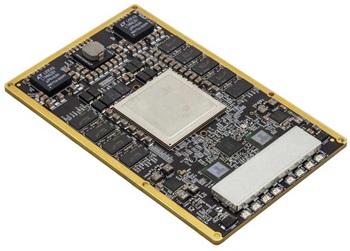
電子戦のアプリケーションや通信アプリケーションの中には、低消費電力で長時間稼働するモバイル・システムが必要とされるものがあります。しかも、そのシステムに必要な主な機能は、スペクトルを監視するための受信機能だけというケースが存在します。本稿では、そのようなアプリケーションを対象とした場合の「ADRV9009-ZU11EG」の評価結果を示します。ADRV9009-ZU11EGは、アナログ・デバイセズがCOTS品として提供しているSOMです(図1)。この製品は集積度が高く、単一のプリント回路基板にトランシーバーIC「ADRV9009」が2つ、「Zynq UltraScale+ MPSoC ZU11EG」(以下、MPSoC)が1つ実装されています。MPSoCは、AMD(Advanced Micro Devices)が提供するマルチプロセッシング対応のSoC(System on Chip)です。以下では、ADRV9009-ZU11EGを単にSOMと呼ぶことにします。.

ADRV9009は、2つのトランスミッタ、2つのレシーバー、2つのオブザベーション・レシーバーを内蔵しています。したがって、SOMは4つの送信チャンネル、4つの受信チャンネル、4つのオブザベーション・レシーバー・チャンネルを備えていることになります。このことから、SOMは様々なユースケースに対応できます。例えば、FR1(Frequency Range 1)に対応する通信機能の実現、MIMO(Multi-input, Multi-output)システムの構築に向けたチャンネル数の拡張、アプリケーションの要件を満たすための消費電力の最小化などに利用することが可能です。表1に、各種の構成でSOMを使用する場合の消費電力を示しました。表中の「チャンネルの構成」は、3つの状態を表しています。「ベースライン」というのは、4送信/4受信のデフォルトの構成に相当します。「中間レベル」は、シンプルに2受信を実現した場合の構成です。「低消費電力」というのは、2受信の構成において消費電力の最小化を図った状態を表します。本稿では、これら3つの構成における消費電力の値を明らかにします。また、それぞれの構成において利用できる機能について解説を加えます。
表1. SOMの構成と消費電力の関係
| チャンネルの構成 | ベースライン | 中間レベル | 低消費電力 |
| 消費電力〔W〕 | 31.5 | 17.2 | 10 |
評価環境の詳細
SOMの評価には、いくつかのハードウェアとソフトウェアが必要です。主要なものを以下に列挙します。
- SOM(ADRV9009-ZU11EG)
- ADRV2CRR-FMC
- WindowsまたはLinuxが稼働するPC
- EVAL-ADP-I2C-USB
- 12V、6ピンの電源
図2に評価環境の概念図を示しました。


ADRV2CRR-FMCはSOMを接続するキャリア・カードです。EVAL-ADP-I2C-USBを使用することにより、SOMが備える電源用のモニタリング/シーケンシングIC「ADM1266」と通信して電源電圧を監視することができます。また、入力電圧の閾値をはじめとする様々なパラメータの値をプログラムすることが可能です。PCは、SOMの評価に用いる各種ツールを利用するための手段となります。代表的なツール(機能)としては、産業用I/Oの信号波形を測定/解析するための「IIO Oscilloscope」、Pythonのライブラリ、イーサネットまたはUART(Universal Asynchronous Receiver/Transmitter)を介した接続の確認機能などが挙げられます。SOMのwikiページには、評価に必要なあらゆる情報が掲載されています。消費電力をはじめ、本稿で示す評価結果は実験室の制御された環境において室温で取得しました。他の環境にSOMを配備する際には、温度の条件を変更して電力の測定/検証を実施する必要があります。
ベースラインの構成における性能
本稿で例にとるSOMは、75MHz~6GHzの周波数に対応します。レシーバーのRF帯域幅は200MHz(A/Dコンバータのサンプル・レートは245.76MSPS)、トランスミッタとオブザベーション・レシーバーのRF帯域幅は最大450MHz(D/Aコンバータのサンプル・レートは491.52MSPS)です。また、このSOMには、MPSoCとデータ処理のためのPS(Processing Subsystem)/PL(Programmable Logic)用のDDR(Double Data Rate)メモリ・バンク、クロック用のジッタ減衰器「HMC7044B」、いくつもの通信インターフェースが実装されています。図3に、SOMのブロック図を示しました。
HMC7044Bは、2つの主要な動作モードをサポートします。SOMのデフォルト(ベースラインに相当)のクロック・アーキテクチャでは、SOM上のHMC7044Bとキャリア・カード上のHMC7044Bを使用することによってマルチチップ同期(MCS:Multichip Sync)を実現します(図4)。ここで言うMCSは、SOMに実装された複数のトランシーバーICの同期をとるための技術です。このクロック・アーキテクチャは、カスケード接続されたクロックIC(HMC7044B)の数に基づいて拡張することが可能です。もう1つのモードは、HMC7044Bが内蔵するPLLをバイパスするクロック分配モードです。クロック・モードの違いについては本稿でも触れますが、HMC7044Bの様々な動作モード、SOMのMCS機能、各モードを使用する場合のトレードオフなどについては、SOMのwikiページを参照してください。
ベースラインのSOMは、4受信、4送信、オブザベーション・レシーバーなしというチャンネル構成で動作します。この構成で初期化時にキャリブレーションを行わず、最高サンプル・レートと最大帯域幅の条件で動作させた場合の消費電力を測定しました。その結果、31.5Wという結果が得られました。システムの消費電力は、SOMに実装されているパワー・マネージメントIC(PMI C)「ADM1177」を使用して測定しました。そのピーク値や谷値によって消費電力のデータに偏りが生じないようにするために、Pythonのスクリプトを使用しました。具体的には、PMICによって消費電力の値を8回取得し、それらの平均値を算出します。このスクリプトについては、SOMのwikiページを参照してください。
消費電力の値を検証するために、ボード上の各能動部品の消費電力を算出すると共に、配電回路網(PDN:Power Distribution Network)を構成するコンポーネントの効率を推定しました。その結果、消費電力が明らかに多いのは、トランシーバーのADRV9009、クロック分配に使用するHMC7044Bと「AD9542」、MPSoCとその補助用回路であることがわかりました。そこで、消費電力を削減するために、これらのIC/回路に注目することにしました。電源電圧、電源レールごとの消費電流(推定値)、レギュレータの動作モードに基づくと、PDNの効率はRF用の電源で約74%、デジタル用の電源で約84%と推定されました。ハードウェアの実装に関するドキュメント、回路図、設計ファイルなど、PDNの詳細についてはSOMのwikiページを参照してください。


比較のために、レシーバー・チャンネルの基本的なRF性能を評価しました。その方法としては、1つのレシーバー・チャンネルに-20dBmの電力レベルの信号(トーン)を入力します。この入力信号は、A/Dコンバータ(ADC)のフルスケールの入力電力に近い値に相当します。信号発生器を使用し、ADRV9009の対応周波数範囲の全体を掃引するように信号を入力しました。得られたデータを基に、基本波と対象周波数範囲内で最大のレベルのスプリアスとの比を計算します。それにより、帯域内のスプリアスフリー・ダイナミック・レンジ(SFDR)の値が得られます。その結果、SFDRの平均値は78.5dBcとなりました。この平均値は、搬送波に対するデシベル値に変換する前の線形なダイナミック・レンジの値を使用して計算されています。
消費電力を削減するための変更
消費電力の最小化は、ハードウェアとソフトウェアに対する変更を組み合わせることによって実現します。基本的なソフトウェアの変更については、IIO Oscilloscopeをはじめとするアナログ・デバイセズのIIO対応ツールを使用します。そうすれば、SDRのパラメータをGUI(Graphical User Interface)によって再設定することができます。IIO Oscilloscopeは、チャンネルのオン/オフの切り替え、初期化時のキャリブレーションやトラッキング・キャリブレーションの有効化/無効化、周波数/帯域幅の再設定、FFT(Fast Fourier Transform)結果のプロットやSPI(Serial Peripheral Interface)で接続したデバイスが備えるレジスタの読み書きといった監視用の機能などを備えています。同様の変更は、Pythonを使って実施することも可能です。ただ、本稿の評価では実装が容易だという理由からIIO Oscilloscopeを使用することにしました。また、HDL(Hardware Description Language)を使用して新たなソフトウェアをコンパイルしてロードすれば、より詳細な変更を実施できます。その方法で設定を行う場合、単に機能をオフにするのではなく、回路を完全に無効化することが可能です。
本稿の最終的な目標は、SOMの2つの受信チャンネルだけを使用する最小限の構成によって消費電力を削減することです。そのことを前提とし、本稿では、まずSOMのベースラインの構成における測定結果と、各種の変更を行った中間レベルの構成における測定結果を比較します。この方法は、様々なユースケースにおける消費電力の推定に利用できます。最初に検討する受信専用の構成は、4つの受信チャンネルから成ります。帯域幅は200MHz、ADCのサンプル・レートは245.76MSPSです。また、トラッキング・キャリブレーションは有効、初期化時のキャリブレーションは無効、オブザベーション・レシーバーは無効に設定しました。トランスミッタは、HDLを使用し、JESDのリンクを完全に削除することによって無効化されています。このシステム構成における消費電力は23.4Wでした。これをベースラインの測定値と比較すると、ADRV9009の全トランスミッタ(JESDを有効にした状態)の消費電力は約8W、トランスミッタ当たりでは約2Wであることがわかります。
どこまで電力を削減できるのかを確認するために、IIOOscilloscopeを使用し、パワーダウン機能によってADRV9009の1つを停止し、2つのレシーバーだけが動作する状態に設定しました。また、回路図上で未使用であることが特定されたHMC7044Bのクロック出力も無効化しました。これらの変更により、システムの消費電力は21.9Wに減少しました。次に、HDLを使用する方法によってJESDのリンクを削除することで、ADRV9009の1つを完全に無効化しました。もう1つのADRV9009については、サンプル・レートを122.88MSPSに下げて、瞬時帯域幅(IBW:Instantaneous Bandwidth)を100MHzに設定し直しました。この構成により、SOMの消費電力は17.2Wとなりました。
続いて、消費電力を更に削減するために、SOMを最小限の動作にとどめた場合に必須ではないのに電力を消費している要素を特定しました。SOMの最小限の動作では、MPSoCはデータの処理に使用されると想定されます。このSOMには、PS用とPL用の2組のDDRチップが実装されています。これらのうち、PS用のDDRはほとんどの場合に使用されます。つまり、SOMの動作に不可欠なものです。一方、PL用のDDRは、ボード上の他のタスクによってPS用のDDRのかなりの部分が使用されている場合に使われます。最小限のチャンネル構成にとどめ、サンプル・レートを低く抑えている状態では、恐らくPL用のDDRチップは必要ありません。そこで、HDLを使用する方法によって同チップを無効化しました。また、USB 3.0、DisplayPort、SGMII(Serial Gigabit Media-Independent Interface)に対応するイーサネット機能などを含むペリフェラルも無効化しました。加えて、クロックICであるAD9542も無効化しました。レギュレータIC「LTM4636」のピンの設定にもいくつかの変更を加えました。更に、パワー・マネージメント・ツール「ADI Power Studio」をEVAL-ADP-I2C-USBと共に使用して過電圧/低電圧の閾値を再プログラムしました。それにより、SOMの入力電圧を5Vに引き下げました。一部のレギュレータは、入力電圧を下げることにより電力損失を低減できるからです。これらの変更を加えることにより、SOMの消費電力は12.8Wまで減少しました。


消費電力を更に削減しなければならないアプリケーションに対応するには、ハードウェアの大幅な変更が必要です。まず、電源については、ピンの設定を変更することでパルス・スキッピング・モードまたはBurst Mode®に設定するとよいでしょう。それにより、消費電流が減少して電源の全体的な効率が向上します。それに加え、MPSoC側のPL_DDRはグラウンドに短絡し、PL用のDDRチップと電源を物理的に取り除きました。また、AD9542、無効化したADRV9009、未使用の水晶発振器も物理的に取り除きます。加えて、未使用のHMC7044BのLVPECL(Low-Voltage Positive Emitter-Coupled Logic)クロックはプルアップし、無効化したコンポーネントにリーク電流が流れ込まないようにしました。HMC7044Bについては、入力周波数を245.76MHzまで下げると共に、クロック分配モードに構成して内部のPLLをバイパスするようにしました。更に、MPSoCのArm®コアの周波数は1.3GHzから300MHzに引き下げました。これらの変更を行った結果、SOMの消費電力は10Wまで減少しました。図5は、ここまでに説明した変更を加えたSOMのブロック図です。
表2は、SOMにおいて多くの電力を消費する要素を列挙し、それぞれの消費電力の推定値を示したものです。ベースラインの構成、中間レベルの構成、ハードウェアとソフトウェアに変更を加えた低消費電力の構成における値をまとめています。
表2. SOMの各要素の消費電力(単位はW)
| デバイス名 | ベースライン | 中間レベル | 低消費電力 |
| XCZU11EG | 5.1 | 5.1 | 3 |
| ADRV9009 | 12.8 | 4.8 | 4.2 |
| HMC7044B | 2.6 | 2.6 | 1.5 |
| DDR4 | 2 | 2 | 1 |
| AD9542 | 1 | 1 | 0 |
| その他 | 8 | 1.7 | 0.3 |
| 合計 | 31.5 | 17.2 | 10 |
表2の「その他」は、システム内のその他すべての消費電力を表しています。これには、その他の能動部品、受動的な電力損失、電源効率などに起因する消費電力が含まれています。上述した変更を加えた後、同じ構成/手法によって帯域内のRFデータを収集しました。その結果、SFDRの平均値は83.1dBcとなり、ベースラインの構成の場合と比べて数dB高くなりました。ただ、これについては低消費電力の構成におけるトレードオフを考慮する必要があります。低消費電力の構成では、HDLを用いることでトランスミッタのJESDリンクが無効化されています。そのため、この構成のSOMはデータ送信の機能を備えていません。また、低消費電力の構成では、PL用のDDRチップを取り除き、HDLを用いて一部のペリフェラルを削除しています。したがって、設定したサンプル・レートでデータをオフロードすることはできません。更に、SOMのクロック・アーキテクチャをクロック分配モードに変更したことによっても大きな影響が生じます。図6に示したのが、新たなクロック・アーキテクチャです。


キャリア・カード上のHMC7044Bは、リファレンスとなる245.76MHzの入力クロックを供給します。一方、SOM上のHMC7044Bは、その入力リファレンス周波数を分周/分配するバッファとして機能します。このモードでは、SOM上のHMC7044Bによってトランシーバーの同期をとることはできません。つまり、SOMを低消費電力の構成にした場合、1つのADRV9009しか使用できず、ボード上のチャンネル数を増やせないことになります。
表3に、ベースラインの構成、中間レベルの構成、低消費電力の構成における機能の相違についてまとめました。
表3. 各構成における機能の相違
| ベースライン | 中間レベル | 低消費電力 | |
| トランスミッタ | あり | なし | なし |
| データのオフロード | 可(複数のインターフェース経由) | 可(複数のインターフェース経由) | 不可(すべての処理をボード上で行う) |
| ボード上のチャンネル数の拡張 | 可 | 可 | 不可 |
表3に示したように、SOMを低消費電力の構成にした場合、HDLを使用することでADRV9009のトランスミッタが無効化されます。つまり、送信機能が存在しない状態になります。また、データをオフロードするための高速インターフェースが無効化されていることに加え、PL用のDDRチップが除去されています。そのため、すべてのデータ処理をSOMのボード上で完結させなければなりません。
まとめ
ADRV9009-ZU11EGは、ソフトウェアとハードウェアの再構成が可能なSOMです。再構成を実施することにより、消費電力に制限がある多くのアプリケーションに対応する形で配備することができます。アナログ・デバイセズのIIOに基づくライブラリやIIO Oscilloscopeなどのツールを活用すれば、使いやすいインターフェースにより、最小限の労力でSOMの消費電力の評価を実施することが可能です。例えば、入力電圧の閾値を引き下げて、SOMのボード上の電源ICの動作モードを変更したとします。そのような手法によってSOMのPDNの効率を最適化すれば、全体的な効率を高められます。また、HDLによって設定を変更する方法を用いれば、サンプル・レートや動作帯域幅を引き下げたり、未使用の機能やペリフェラルを無効化したりすることが可能になります。そうすれば、ハードウェアを変更することなく消費電力を更に削減できます。アプリケーションにおいて消費電力を最小化することが必須である場合、上記の変更とハードウェアの大幅な変更を組み合わせることにより消費電力を大幅に削減できます。但し、ボード上でチャンネル数を拡張するなど、SOMが元々備えている機能の大半は利用できなくなります。この点には注意が必要です。
参考資料
ADRV9009-ZU11EG RF System-on-Module(RFに対応するSOM「ADRV9009-ZU11EG」)、Analog Devices
