LT83401
新規設計に推奨42V、1A/2.5A、降圧Silent Switcher 3、超低ノイズ・リファレンス付き
- 製品モデル
- 4
- 1Ku当たりの価格
- 最低価格:$2.49
製品情報
- Silent Switcher®(サイレント・スイッチャ)3アーキテクチャ
- 超低RMSノイズ(10Hz~100kHz):2.8μVRMS
- 超低スポット・ノイズ:4nV/√Hz(10kHz時)
- 超低EMI放射
- 超高速過渡応答
- 出力容量を最小化
- 高周波で高い効率性
- 2MHz、12VIN~5VOUTで最大92.4%の効率
- 入力電圧範囲:2.8V~42V
- 出力電圧範囲:0V~(VIN - 1V)
- 最大15VOUTのユニティ・ゲイン構成
- 高速最小スイッチオン時間:22ns
- 精密リファレンス:リモート・センス付きの場合、全温度範囲で±0.8%
- 強制連続モード機能
- 調整と同期が可能:300kHz~6MHz
- 設定可能なパワー・グッド
- 小型の15ピン3mm x 2mm LFCSPパッケージ
- ピン互換ファミリ:LT83201(18V、1A)、LT83203(18V、3A)、LT83205(18V、5A)
- AEC-Q100認定を申請中
LT®83401/LT®83402同期整流式降圧レギュレータは、超低ノイズ・リファレンスとSilent Switcherアーキテクチャを組み合わせた独自の設計により、高効率と優れた広帯域ノイズ性能の両方を実現します。
革新的な超低ノイズ・アーキテクチャにより、スイッチング・レギュレータで非常に低い周波数(0.1Hz~100kHz)の出力ノイズ性能が得られます。出力電圧を単一の抵抗で設定できるため、出力電圧に関係なく出力ノイズがほぼ一定になります。
Silent Switcherアーキテクチャは、高スイッチング周波数で高い効率を実現しながら、電磁場干渉(EMI)放射を最小限に抑えます。
LT83401/LT83402は、同期スイッチング・レギュレータの高い変換効率によって効果が得られる、ノイズの影響を受けやすい大電流アプリケーションに適しています。
アプリケーション
- 自動車用および産業用電源
- 医療用アプリケーション:イメージングと診断
- 高速かつ高精度のデータ・コンバータ
- バイポーラ超低ノイズ電源
- 低ノイズの計測器とディスプレイ
ドキュメント
データシート 2
ユーザ・ガイド 1
| 製品モデル | ピン/パッケージ図 | 資料 | CADシンボル、フットプリント、および3Dモデル |
|---|---|---|---|
| LT83401RUDB#TRMPBF | LFCSP | ||
| LT83401RUDB#TRPBF | LFCSP | ||
| LT83401RUDB#WTRMPBF | LFCSP | ||
| LT83401RUDB#WTRPBF | LFCSP |
| 製品モデル | 製品ライフサイクル | PCN |
|---|---|---|
|
3 20, 2026 - 26_0080 LT83401/2 Data Sheet EC Table Specification Change |
||
| LT83401RUDB#TRMPBF | 製造中 | |
| LT83401RUDB#TRPBF | 製造中 | |
| LT83401RUDB#WTRMPBF | 製造中 | |
| LT83401RUDB#WTRPBF | 製造中 | |
これは最新改訂バージョンのデータシートです。
ソフトウェア・リソース
必要なソフトウェア/ドライバが見つかりませんか?
ドライバ/ソフトウェアをリクエストツールおよびシミュレーション
LTspice
下記製品はLTspiceで使用することが出来ます。:
- LT83401
LTpowerCAD
次のデバイス用の設計ツールがLTpowerCADでご使用になれます。
- LT83401
LTspice®は、無料で提供される強力で高速な回路シミュレータと回路図入力、波形ビューワに改善を加え、アナログ回路のシミュレーションを容易にするためのモデルを搭載しています。
評価用キット
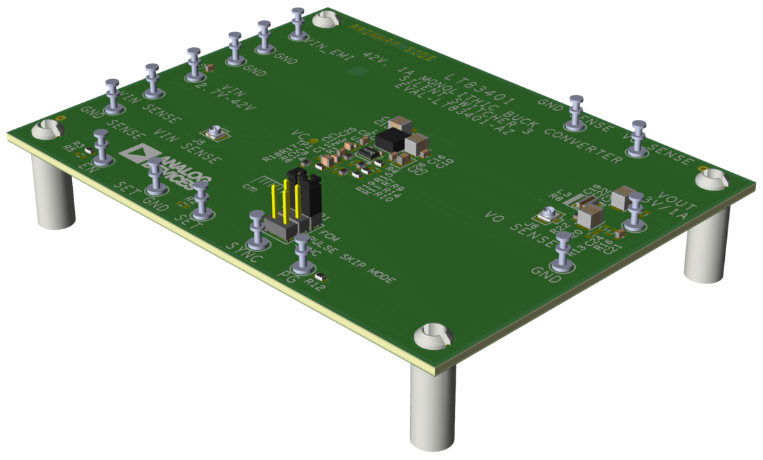
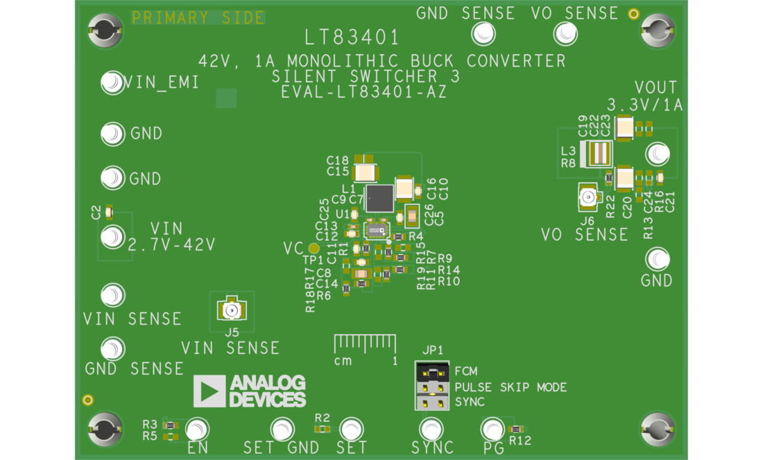
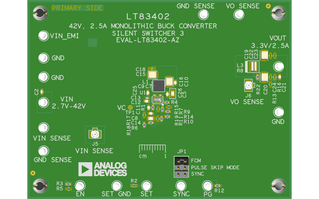
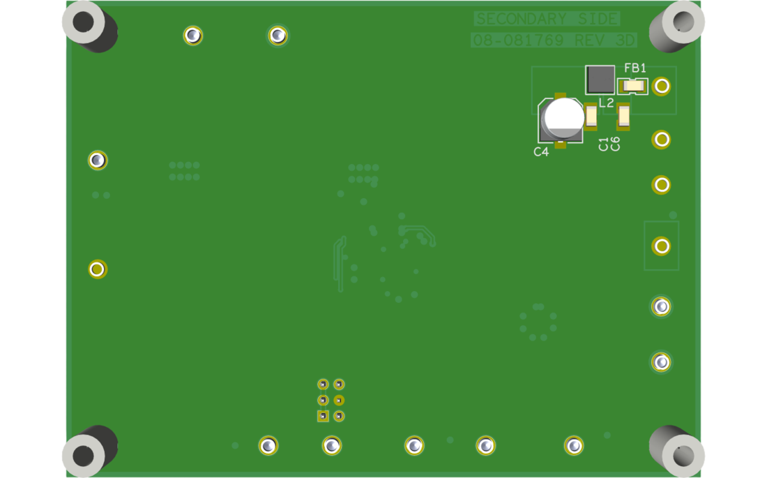
42V、1A/2.5A、降圧Silent Switcher 3、超低ノイズ・リファレンス付き
資料
最新のディスカッション
LT83401に関するディスカッションはまだありません。意見を投稿しますか?
EngineerZone®でディスカッションを始める