ADPL31613

発売前

Dual 1.3A, 1.2MHz Boost/Inverter in 3mm × 3mm DFN

Viewing:
利用上の注意

本データシートの英語以外の言語への翻訳はユーザの便宜のために提供されるものであり、リビジョンが古い場合があります。最新の内容については、必ず最新の英語版をご参照ください。

なお、日本語版のデータシートは基本的に「Rev.0」(リビジョン0)で作成されています。そのため、英語版が後に改訂され、複数製品のデータシートがひとつに統一された場合、同じ「Rev.0」の日本語版のデータシートが異なる製品のデータシートとして表示されることがあります。たとえば、「ADM3307E」の場合、日本語データシートをクリックすると「ADM3311E」が表示されます。これは、英語版のデータシートが複数の製品で共有できるように1本化され、「ADM3307E/ADM3310E/ADM3311E/ADM3312E/ADM3315E」(Rev.J)と改訂されたからで、決して誤ってリンクが張られているわけではありません。和文化されたデータシートを少しでも有効に活用していただくためにこのような方法をとっておりますので、ご了解ください。

アナログ・デバイセズ社は、提供する情報が正確で信頼できるものであることを期していますが、その情報の利用に関して、あるいはその利用によって生じる第三者の特許やその他の権利の侵害に関して一切の責任を負いません。また、アナログ・デバイセズ社の特許または特許の権利の使用を明示的または暗示的に許諾するものでもありません。仕様は予告なしに変更する場合があります。本紙記載の商標および登録商標は、各社の所有に属します。

製品情報

  • 1.2MHz Switching Frequency
  • Low VCESAT Switches: 380mV at 1.3A
  • High Output Voltage: Up to 38V
  • Wide Input Range: 2.4V to 16V
  • Inverting Capability
  • 5V at 630mA from 3.3V Input
  • 12V at 320mA from 5V Input
  • –12V at 200mA from 5V Input
  • Uses Tiny Surface-Mount Components
  • Low Shutdown Current: <2μA
  • Low Profile (0.75mm) 10-Lead 3mm × 3mm Dual Flat No-Lead (DFN) Package
ADPL31613
Dual 1.3A, 1.2MHz Boost/Inverter in 3mm × 3mm DFN
ADPLl31613 Typical Application ADPLl31613 Typical Application Efficiency ADPL31613 Pin Configuration ADPL31613 Chip Illustration
myAnalogに追加

myAnalogの製品セクション(通知受け取り)、既存/新規プロジェクトに製品を追加する。

新規プロジェクトを作成
質問する
サポート

アナログ・デバイセズのサポート・ページはアナログ・デバイセズへのあらゆるご質問にお答えするワンストップ・ポータルです。


ドキュメント

さらに詳しく
myAnalogに追加

myAnalogのリソース・セクション、既存/新規プロジェクトにメディアを追加する。

新規プロジェクトを作成

ソフトウェア・リソース

必要なソフトウェア/ドライバが見つかりませんか?

ドライバ/ソフトウェアをリクエスト

ツールおよびシミュレーション

LTspice


下記製品はLTspiceで使用することが出来ます。:

  • ADPL31613
LTspice

LTspice®は、無料で提供される強力で高速な回路シミュレータと回路図入力、波形ビューワに改善を加え、アナログ回路のシミュレーションを容易にするためのモデルを搭載しています。


評価用キット
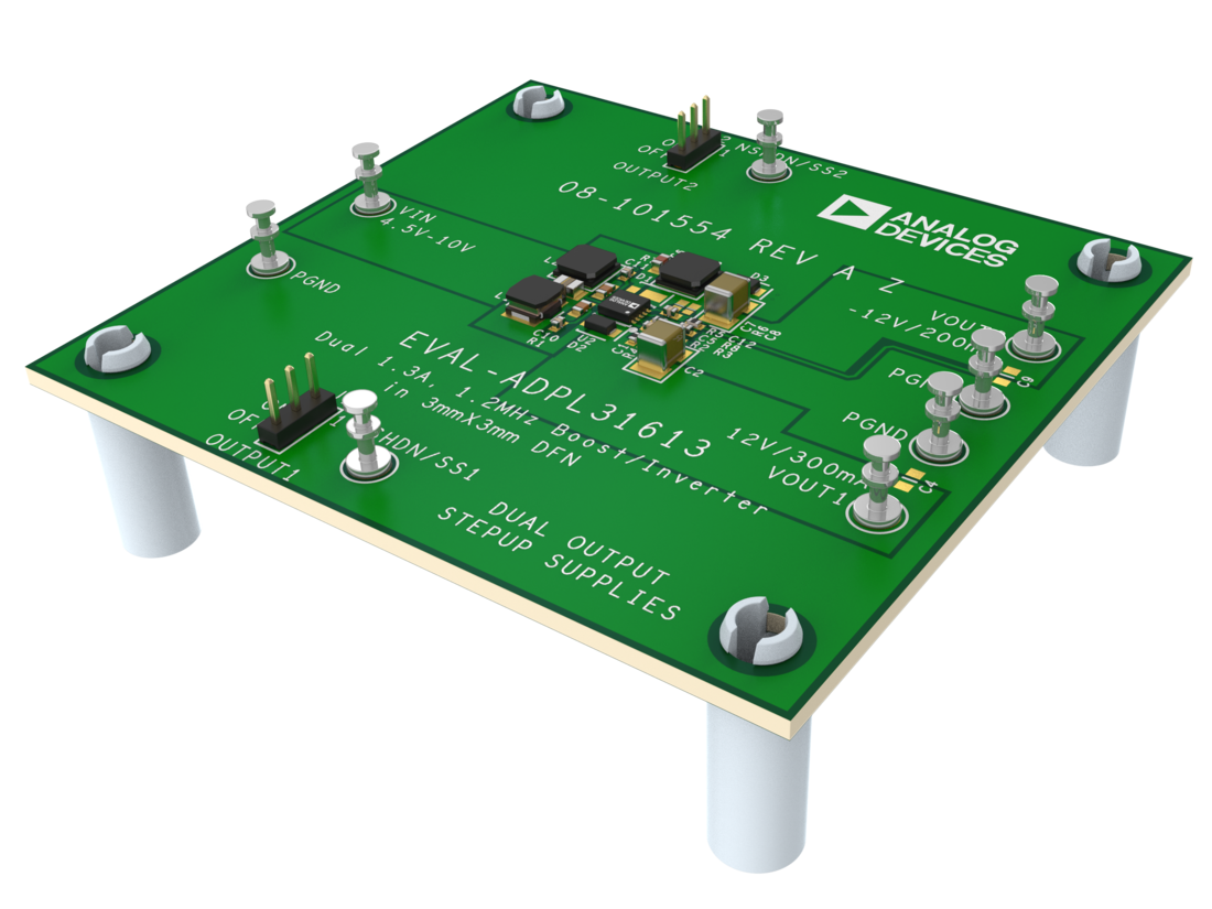
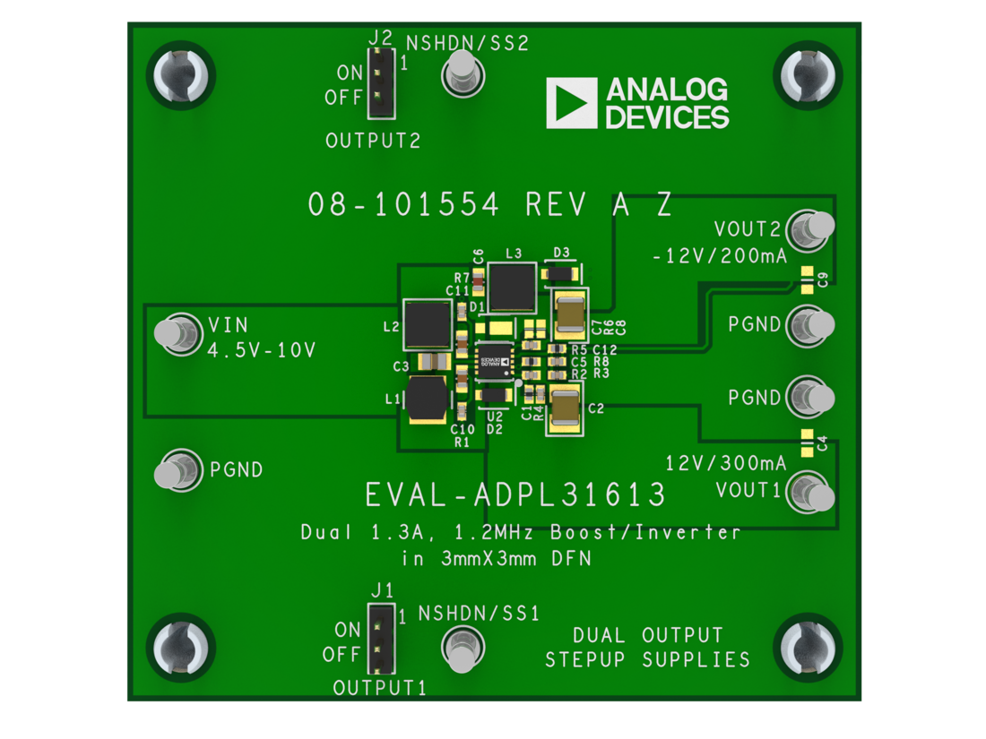
eval board
EVAL-ADPL31613-AZ

Evaluates: ADPL31613 in a ±12V Output Voltage Application

機能と利点

  • VOUT1 = 12V at IOUT1 = up to 300mA
  • VOUT2 = -12V at IOUT = up to 200mA
  • VIN Range = 4.5V to 10V
  • Fixed Frequency 1.2MHz Operation
  • Resistor Programmable Output Voltage
  • Current Mode Control, Internal Compensation and Soft-Start
  • Proven Printed Circuit Board (PCB) Layout
  • Fully Assembled and Tested

製品詳細

The EVAL-ADPL31613-AZ evaluation board is a dual-output converter featuring the ADPL31613 in both boost and inverter configurations. Both converters are powered from the same 4.5V to 10V input source. The Boost converter outputs 12V at 300mA, and the Inverter outputs -12V at 200mA. The evaluation board demonstrates small size and a low component count. The ADPL31613 operates with inputs up to 16V, but on this evaluation circuit the input is limited by the boost output magnitude. In a Boost converter, the input needs to be less than the output.

The EVAL-ADPL31613-AZ is designed so that the Inverting converter can be easily configured as a Boost converter. Instructions are included in the EVAL-ADPL31613-AZ Schematic Diagram. Both circuits are designed to demonstrate the soft-start feature, the advantages of the 1.2MHz switching frequency, and the internal 38V/1.3A switches.

Both outputs of this evaluation board can be modified to handle higher voltages. The evaluation board is intended for space-conscious applications such as digital cameras, cellular phones, palmtop computers, PC cards, miniature disk drives, X Digital Subscriber Line (xDSL) power supplies, flash memory products, local 5V or 12V supplies, and Liquid-Crystal Display (LCD) displays.

EVAL-ADPL31613-AZ
Evaluates: ADPL31613 in a ±12V Output Voltage Application
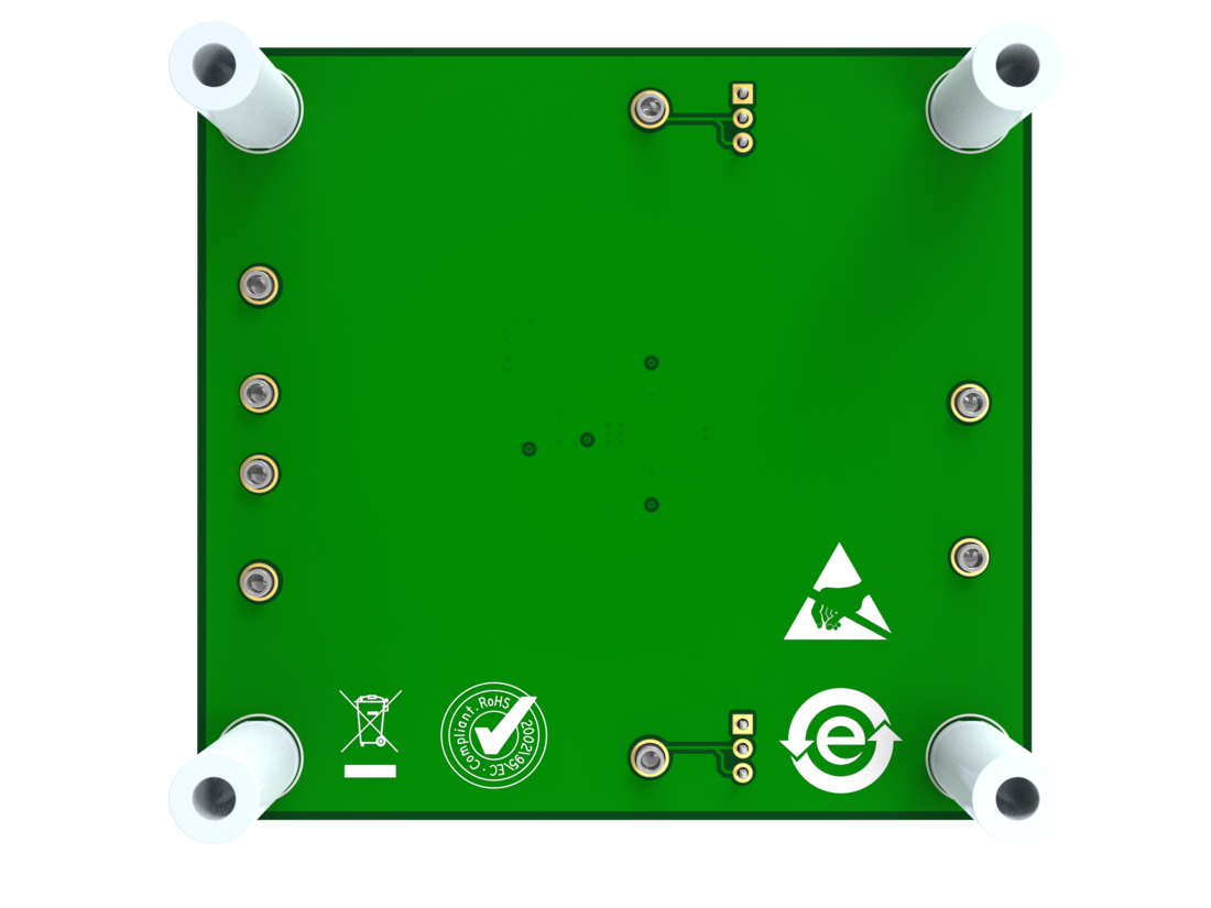
EVAL-ADPL31613-AZ Top Angle Evaluation Board EVAL-ADPL31613-AZ Top Evaluation Board EVAL-ADPL31613-AZ Bottom Evaluation Board

最新のディスカッション

ADPL31613に関するディスカッションはまだありません。意見を投稿しますか?

EngineerZone®でディスカッションを始める

最近表示した製品