ADF4382A
新規設計に推奨高性能コンバータのクロック供給アプリケーション向け、2.87GHz~21GHzフラクショナルN PLL/VCO
高性能コンバータのクロック供給アプリケーション向け、2.87GHz~21GHzフラクショナルN PLL/VCO
- 製品モデル
- 2
- 1Ku当たりの価格
- 最低価格:$184.58
製品情報
- 基本出力周波数範囲:11.5GHz~21GHz
- 2分周出力周波数範囲:5.75GHz~10.5GHz
- 4分周出力周波数範囲:2.875GHz~5.25GHz
- 20GHzでの積分RMSジッタ = 20fs(積分帯域幅:100Hz~100MHz)
- 20GHzでの積分RMSジッタ = 31fs(ADC S/N比法)
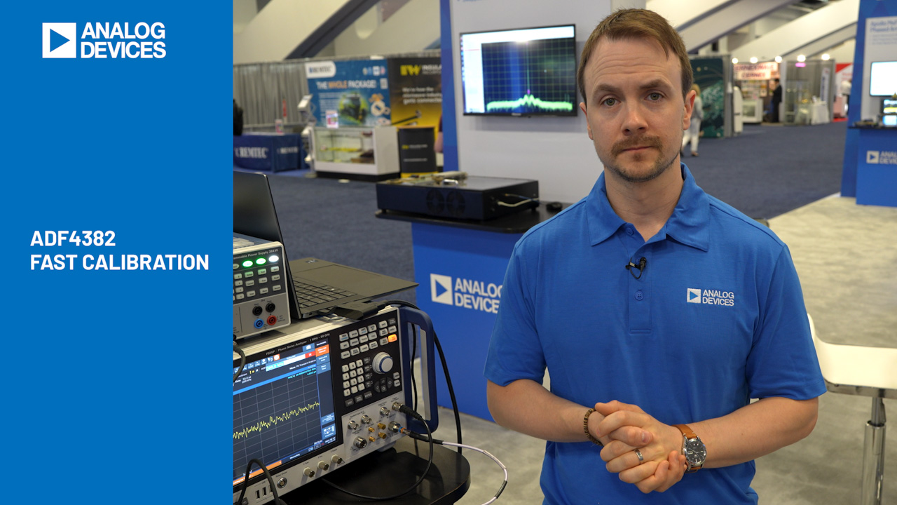
- VCO高速キャリブレーション時間:1μs未満
- VCO自動キャリブレーション時間:100μs未満
- 位相ノイズ・フロア:20GHzで−156dBc/Hz
- PLL仕様
- −239dBc/Hz:正規化された帯域内位相ノイズ・フロア
- −287dBc/Hz:正規化された1/f位相ノイズ・フロア
- 最大位相/周波数検出器入力周波数:625MHz
- リファレンス入力周波数:4.5GHz
- fPFDスプリアス(代表値):−90dBc
- リファレンスと出力の間の遅延仕様
- 伝搬遅延の温度係数:0.06ps/°C
- 調整ステップ・サイズ:1ps未満
- マルチチップ出力位相アライメント
- 3.3Vおよび5Vの電源
- ADIsimPLL™ループ・フィルタ設計ツール対応
- 7mm × 7mm、48端子LGA
- 動作温度範囲:−40°C~+105°C
ADF4382Aは、高性能、超低ジッタのフラクショナルNフェーズ・ロック・ループ(PLL)です。電圧制御発振器(VCO)を内蔵しており、データ・コンバータ・クロック・アプリケーションまたは5Gアプリケーションの局所発振器(LO)生成に適しています。この高性能PLLは、−239dBc/Hzの性能指数、低い1/fノイズ、および高いPFD周波数(インテジャー・モードで625MHz)を持ち、極めて小さい帯域内ノイズと積分ジッタを実現できます。ADF4382Aは11.5GHz~21GHzの基本オクターブ範囲で周波数を生成できるため、低調波フィルタが不要になります。ADF4382Aの2分周出力分周器と4分周出力分周器により、それぞれ5.75GHz~10.5GHz、2.875GHz~5.25GHzの周波数を生成できます。
複数のデータ・コンバータ・クロック・アプリケーションの場合、ADF4382Aは、PLLフィードバック・ループに出力分周器を含めることにより、入力リファレンス・エッジに合わせて出力を自動的に調整します。確定的遅延や遅延調整機能が要求されるアプリケーションに対応するために、リファレンスと出力との間の遅延を1ps未満の分解能で調整することができます。複数のデバイスや温度変化に対してリファレンスと出力の間の遅延が維持されるため、予測可能かつ高精度なマルチチップ・アライメントが実現します。
ADF4382Aのブロック図はシンプルです。単純化されたシリアル・ペリフェラル・インターフェース(SPI)レジスタ・マップ、外部SYNC入力、更にインテジャー・モードとフラクショナル・モードの両方で繰り返し可能なマルチチップ・アライメントによって開発時間を短縮できます。
アプリケーション
- 高性能データ・コンバータのクロック供給
- ワイヤレス・インフラストラクチャ(MC-GSM、5G、6G)
- 試験および計測
ドキュメント
データシート 2
アプリケーション・ノート 1
技術記事 1
ビデオ 1
デバイス・ドライバ 2
| 製品モデル | ピン/パッケージ図 | 資料 | CADシンボル、フットプリント、および3Dモデル |
|---|---|---|---|
| ADF4382ABCCZ | 48-Terminal Land Grid Array [LGA] (7mm x 7mm x 1.25 mm) | ||
| ADF4382ABCCZ-RL7 | 48-Terminal Land Grid Array [LGA] (7mm x 7mm x 1.25 mm) |
これは最新改訂バージョンのデータシートです。
ソフトウェア・リソース
評価用ソフトウェア 0
必要なソフトウェア/ドライバが見つかりませんか?
ハードウェア・エコシステム
ツールおよびシミュレーション
IBISモデル 1
ADIsimPLL™
ADIsimPLLは、アナログ・デバイセズの新しい高性能PLL製品の迅速で信頼性の高い評価を可能にします。これは、現在利用できる最も包括的なPLLシンセサイザ設計およびシミュレーション・ツールです。実施されるシミュレーションには、PLL性能に影響を与える重要な非線形効果がすべて含まれます。ADIsimPLLは、設計プロセスから1回以上の反復作業を削除し、設計から市場投入までの時間を短縮します。
ツールを開く
LTspice®は、無料で提供される強力で高速な回路シミュレータと回路図入力、波形ビューワに改善を加え、アナログ回路のシミュレーションを容易にするためのモデルを搭載しています。
評価用キット


