ADL8130

新規設計に推奨

GaAs, pHEMT, MMIC, 0.01GHz to 8GHz, Low Noise Amplifier

Viewing:
利用上の注意

本データシートの英語以外の言語への翻訳はユーザの便宜のために提供されるものであり、リビジョンが古い場合があります。最新の内容については、必ず最新の英語版をご参照ください。

なお、日本語版のデータシートは基本的に「Rev.0」(リビジョン0)で作成されています。そのため、英語版が後に改訂され、複数製品のデータシートがひとつに統一された場合、同じ「Rev.0」の日本語版のデータシートが異なる製品のデータシートとして表示されることがあります。たとえば、「ADM3307E」の場合、日本語データシートをクリックすると「ADM3311E」が表示されます。これは、英語版のデータシートが複数の製品で共有できるように1本化され、「ADM3307E/ADM3310E/ADM3311E/ADM3312E/ADM3315E」(Rev.J)と改訂されたからで、決して誤ってリンクが張られているわけではありません。和文化されたデータシートを少しでも有効に活用していただくためにこのような方法をとっておりますので、ご了解ください。

アナログ・デバイセズ社は、提供する情報が正確で信頼できるものであることを期していますが、その情報の利用に関して、あるいはその利用によって生じる第三者の特許やその他の権利の侵害に関して一切の責任を負いません。また、アナログ・デバイセズ社の特許または特許の権利の使用を明示的または暗示的に許諾するものでもありません。仕様は予告なしに変更する場合があります。本紙記載の商標および登録商標は、各社の所有に属します。

製品情報

  • High gain: 25.5dB typical from 0.01GHz to 2GHz
  • Low noise figure: <0.6dB typical from 0.5GHz to 2GHz
  • Power-down voltage pin (VPD) for enabling and disabling the amplifier
  • Single-supply bias
  • Extended operating temperature range: −55°C to +125°C
  • RoHS-compliant, 2mm × 2mm, 8-lead LFCSP
ADL8130
GaAs, pHEMT, MMIC, 0.01GHz to 8GHz, Low Noise Amplifier
ADL8130 Functional Block Diagram ADL8130 Pin Configuration
myAnalogに追加

myAnalogの製品セクション(通知受け取り)、既存/新規プロジェクトに製品を追加する。

新規プロジェクトを作成
質問する
サポート

アナログ・デバイセズのサポート・ページはアナログ・デバイセズへのあらゆるご質問にお答えするワンストップ・ポータルです。


ドキュメント

さらに詳しく
myAnalogに追加

myAnalogのリソース・セクション、既存/新規プロジェクトにメディアを追加する。

新規プロジェクトを作成

ソフトウェア・リソース

必要なソフトウェア/ドライバが見つかりませんか?

ドライバ/ソフトウェアをリクエスト

ツールおよびシミュレーション

Sパラメータ 1


評価用キット

eval board
EVAL-ADL8130

Evaluating the ADL8130 GaAs, pHEMT, MMIC, 0.01GHz to 8GHz, Low Noise Amplifier

機能と利点

  • 4-layer, Rogers 4003C evaluation board
  • End launch, 2.9mm RF connectors
  • Through calibration path (depopulated connectors)

製品詳細

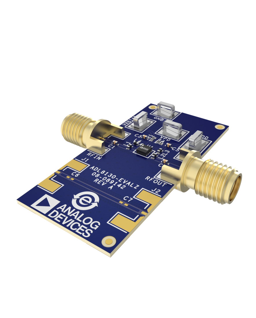
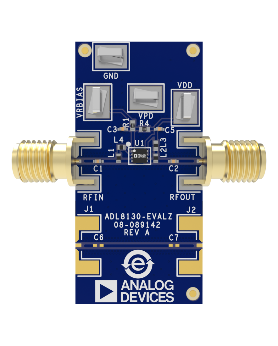
The ADL8130-EVALZ is a 4-layer printed circuit board (PCB) fabricated from 0.254mm (10mil) thick, Rogers 4003C, copper clad, forming a nominal thickness of 1.58mm (62mils). The ADL8130- EVALZ is designed to operate from 0.01GHz to 8GHz. The RFIN and RFOUT ports on the ADL8130-EVALZ are populated with 2.9mm, female coaxial connectors. The ADL8130-EVALZ is populated with components suitable for use over the entire −55°C to +125°C operating temperature range.

To calibrate out board trace losses, a through calibration path is provided between the J1 and J2 connectors. J1 and J2 must be populated with RF connectors to use the through calibration path. Refer to Figure 5 and Table 1 in user guide for the through calibration path performance for the ADL8130-EVALZ.

Access the ADL8130-EVALZ ground and drain voltage through the surface-mount technology (SMT) test point connectors, GND and VDD. A supplementary test point for VRBIAS is included for simple access on the RBIAS pin (see Figure 6 and Figure 7 in user guide for the test point locations).

The RF traces on the ADL8130-EVALZ are 50Ω, grounded, coplanar waveguide. The package ground leads and the exposed pad connect directly to the ground plane. Multiple vias connect the top and bottom ground planes with particular focus on the area directly beneath the ground paddle to provide adequate electrical conduction and thermal conduction.

The power supply decoupling capacitors on the ADL8130-EVALZ represent the configuration used to characterize and qualify the device.

For full details on the ADL8130, see the ADL8130 data sheet, which must be consulted in conjunction with this user guide when using the ADL8130-EVALZ.

EVAL-ADL8130
Evaluating the ADL8130 GaAs, pHEMT, MMIC, 0.01GHz to 8GHz, Low Noise Amplifier
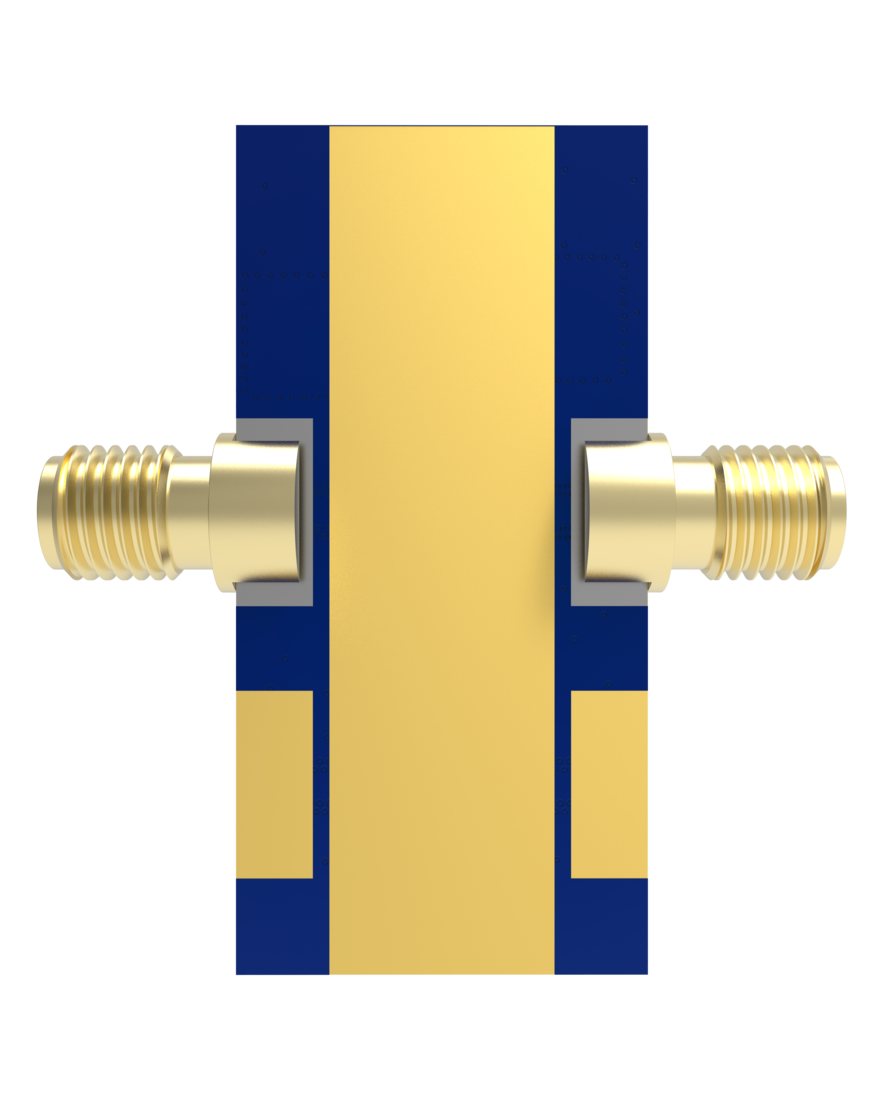
ADL8130-EVALZ Top Angle Evaluation Board ADL8130-EVALZ Top Evaluation Board ADL8130-EVALZ Bottom Evaluation Board

最新のディスカッション

ADL8130に関するディスカッションはまだありません。意見を投稿しますか?

EngineerZone®でディスカッションを始める

最近表示した製品