ADL8100

新規設計に推奨

GaAs, pHEMT, MMIC, Low Noise Amplifier, 0.01 GHz to 20 GHz

利用上の注意

本データシートの英語以外の言語への翻訳はユーザの便宜のために提供されるものであり、リビジョンが古い場合があります。最新の内容については、必ず最新の英語版をご参照ください。

なお、日本語版のデータシートは基本的に「Rev.0」(リビジョン0)で作成されています。そのため、英語版が後に改訂され、複数製品のデータシートがひとつに統一された場合、同じ「Rev.0」の日本語版のデータシートが異なる製品のデータシートとして表示されることがあります。たとえば、「ADM3307E」の場合、日本語データシートをクリックすると「ADM3311E」が表示されます。これは、英語版のデータシートが複数の製品で共有できるように1本化され、「ADM3307E/ADM3310E/ADM3311E/ADM3312E/ADM3315E」(Rev.J)と改訂されたからで、決して誤ってリンクが張られているわけではありません。和文化されたデータシートを少しでも有効に活用していただくためにこのような方法をとっておりますので、ご了解ください。

アナログ・デバイセズ社は、提供する情報が正確で信頼できるものであることを期していますが、その情報の利用に関して、あるいはその利用によって生じる第三者の特許やその他の権利の侵害に関して一切の責任を負いません。また、アナログ・デバイセズ社の特許または特許の権利の使用を明示的または暗示的に許諾するものでもありません。仕様は予告なしに変更する場合があります。本紙記載の商標および登録商標は、各社の所有に属します。

Viewing:

製品情報

  • Low noise figure: 2.5 dB typical at 6 GHz to 14 GHz
  • Single positive supply (self biased)
  • High gain: 20 dB typical from 0.01 GHz to 6 GHz
  • High OIP3: 38 dBm typical from 0.01 GHz to 6 GHz
  • RoHS-compliant, 2 mm × 2 mm, 8-lead LFCSP

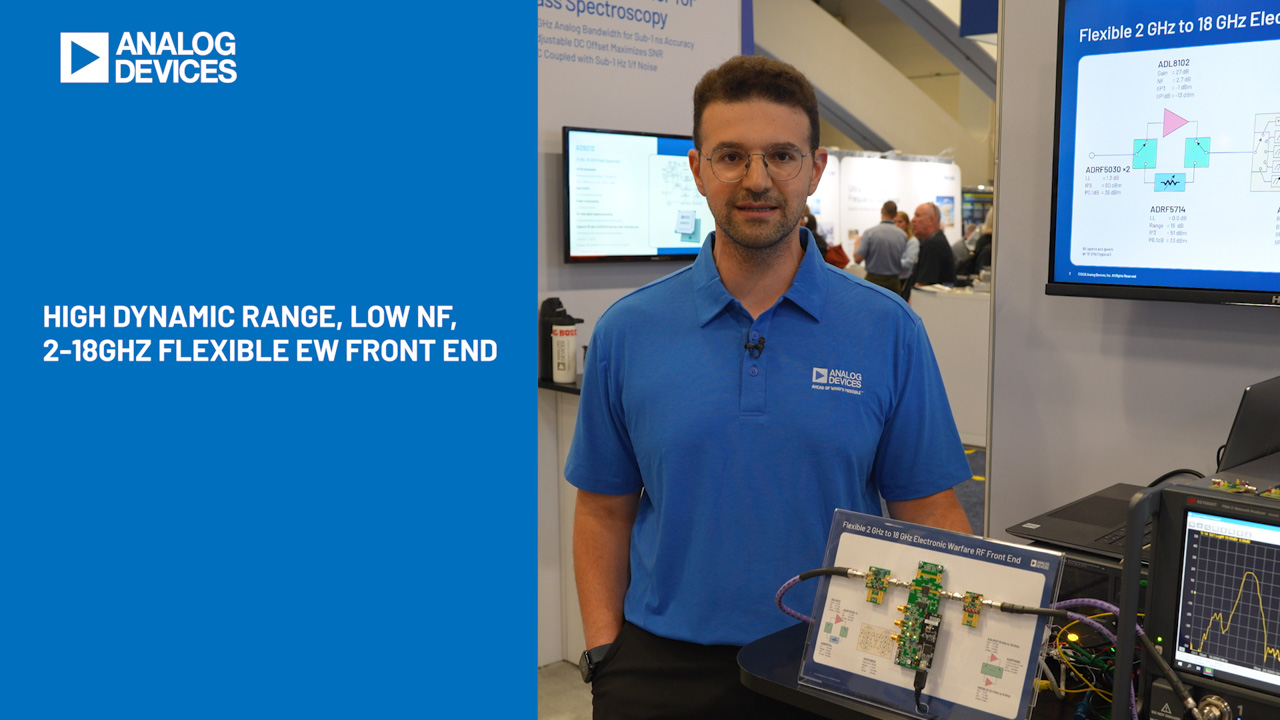
The ADL8100 is a gallium arsenide (GaAs), monolithic microwave integrated circuit (MMIC), pseudomorphic high electron mobility transistor (pHEMT), wideband low noise amplifier (LNA) that operates from 0.01 GHz to 20 GHz. The ADL8100 provides a typical gain of 20 dB at 0.01 GHz to 6 GHz, a 2.5 dB typical noise figure at 6 GHz to 14 GHz, and a typical output third-order intercept (OIP3) of 38 dBm at 0.01 GHz to 6 GHz, requiring only 220 mA from a 5 V supply voltage. The power dissipation can be lowered at the expense of OIP3 and output power. The ADL8100 also features inputs and outputs that are DC-coupled and internally matched to 50 Ω.

The ADL8100 is housed in a RoHS-compliant, 2 mm × 2 mm, 8-lead LFCSP.

APPLICATIONS

  • Satellite communication
  • Telecommunications
  • Civilian radars
  • Military radars
  • Weather radars
  • Electronic warfare
  • ADL8100
    GaAs, pHEMT, MMIC, Low Noise Amplifier, 0.01 GHz to 20 GHz
    ADL8100 -  Functional Block Diagram ADL8100 - Pin Configuration
    myAnalogに追加

    myAnalogの製品セクション(通知受け取り)、既存/新規プロジェクトに製品を追加する。

    新規プロジェクトを作成
    質問する
    サポート

    アナログ・デバイセズのサポート・ページはアナログ・デバイセズへのあらゆるご質問にお答えするワンストップ・ポータルです。


    ドキュメント

    さらに詳しく
    myAnalogに追加

    myAnalogのリソース・セクション、既存/新規プロジェクトにメディアを追加する。

    新規プロジェクトを作成

    ソフトウェア・リソース

    必要なソフトウェア/ドライバが見つかりませんか?

    ドライバ/ソフトウェアをリクエスト

    ツールおよびシミュレーション

    Sパラメータ 1


    評価用キット

    eval board
    EVAL-ADL8100

    Evaluating the ADL8100 GaAs, pHEMT, MMIC, Low Noise Amplifier, 0.01 GHz to 20 GHz

    機能と利点

  • 2-layer Rogers 4350B evaluation boards with heat spreaders
  • End launch, 2.9 mm RF connectors
  • Through calibration path (depopulated connectors)
  • 製品詳細

    The ADL8100ACPZN-EVALZ and ADL8100ACPZN-EVAL1Z are 2-layer printed circuit boards (PCB) fabricated from 10 mil thick, Rogers 4350B, copper clad, mounted to an aluminum heat spreader. The heat spreader assists in providing thermal relief to the device as well as mechanical support to the PCB. Mounting holes on the heat spreader allow attachment to larger heat sinks for improved thermal management.

    The RFIN and RFOUT ports on the ADL8100ACPZN-EVALZ and ADL8100ACPZN-EVAL1Z are populated with 2.9 mm, female coaxial connectors, and the respective RF traces have a 50 Ω characteristic impedance. The ADL8100ACPZN-EVALZ and ADL8100ACPZN-EVAL1Z are populated with components suitable for use over the entire −40°C to +85°C operating temperature range.

    To calibrate out board trace losses, a through calibration path, THRUCAL, is provided between the THRUCAL connectors (J1 and J2). THRUCAL must be populated with RF connectors to use the through calibration path.

    The power voltages and ground path are accessed through surface- mounted technology (SMT) test points.

    An external wideband bias tee must be connected to RFOUT of the ADL8100ACPZN-EVALZ to provide bias current and AC coupling on RFOUT. The BT2-0040 from Marki Microwave is recommended. The ADL8100ACPZN-EVAL1Z has an on-board SMT bias tee.

    For full details on the ADL8100, see the ADL8100 data sheet, which must be consulted in conjunction with the user guide when using the ADL8100ACPZN-EVALZ and ADL8100ACPZN-EVAL1Z.

    ADXBAND16EBZ

    16Tx/16Rx Direct X-Band Sampled Phased-Array/RADAR/SATCOM Development Platform

    機能と利点

    ADXBAND16EBZ Digitizing Card
    • Multi-Channel, Wideband System Development Platform Using Apollo (AD9084)
    • Mates With Xilinx VCU118 Evaluation Board (Not Included)
    • 16x RF Receive (Rx) Channels
      • Total 16x 8GSPS to 20GSPS ADC
      • Digital Down Converters (DDCs), Each Including Complex Numerically-Controlled Oscillators (NCOs)
      • Programmable Finite Impulse Response Filters (pFIRs)
      • Complex Finite Impulse Response Filters (CFIRs)
    • 16x RF Transmit (Tx) Channels
      • Total 16x 8GSPS to 28GSPS DAC
      • Digital Up Converters (DUCs), Each Including Complex Numerically-Controlled Oscillators (NCOs)
      • Programmable Finite Impulse Response Filters (pFIRs)
      • Complex Finite Impulse Response Filters (CFIRs)
    • Flexible Rx & Tx RF Front-Ends
      • Rx: Filtering, Amplification, Digital Step Attenuation for Gain Control
      • Tx: Filtering, Amplification
    • Flexible Clock Distribution
      • On-Board Clock Distribution from Single External 400MHz Reference
      • Support for External Converter Clock per AD9084 via solder rework
    • On-Board Power Regulation from Single 12V Power Adapter (Included)
    16Tx / 16Rx Calibration Board
    • Mates to ADXBAND16EBZ Digitizing Card & VCU118 PMOD Interface (Cable Included)
    • Provides Both Individual Adjacent Channel Loopback and Combined Channel Loopback Options
    • Combined Tx Channels Out Option
    • Combined Rx Channels In Option
    Software Features and Benefits

    Easy Control Tools and Platform Interfaces to Simplify Software Framework Developments:

    • IIO Oscilloscope GUI
    • MATLAB Add-Ons & Example Scripts
    • Example HDL Builds including JESD204C Bring-Up
    • Embedded Software Solutions for Linux and Device Drivers
    Software Reference Design Examples for ADEF Applications to Reduce Prototyping Time:
    • Multi-Chip Synchronization for Power-Up Phase Determinism
    • System-Level Amplitude/Phase Alignment Using NCOs
    • Low-Latency ADC-to-DAC Loopback Bypassing JESD Interface
    • pFIR Control for Broadband Channel-to-Channel Amplitude/Phase Alignment
    • Fast-Frequency Hopping

    製品詳細

    The ADXBAND16EBZ contains four AD9084 mixed‑signal front‑end devices, including the RF front end, clocking, and power circuitry. The ADXBAND16EBZ serves as a complete system solution targeting common applications such as phased‑array radars, wideband systems, and ground‑based SATCOM. Its primary target application is a 16‑Tx/16‑Rx direct X‑band sampling phased array.

    The platform is intended as a testbed for demonstrating multi‑chip synchronization, as well as implementing system‑level calibrations, beamforming algorithms, and other signal‑processing techniques. The system is designed to interface with the VCU118 Evaluation Board from Xilinx®, which features the Virtex® UltraScale+™ XCVU9P FPGA, along with provided reference software, HDL code, and MATLAB system‑level interfaces.

    A 16‑Tx/16‑Rx Calibration Board can be used to develop system‑level calibration algorithms, including demonstrations of power‑up phase determinism. The Calibration Board provides improvements in combined‑channel dynamic range, spurious performance, and phase noise, and can be controlled via a MATLAB add‑on when connected to the PMOD interface of the VCU118.

    EVAL-ADL8100
    Evaluating the ADL8100 GaAs, pHEMT, MMIC, Low Noise Amplifier, 0.01 GHz to 20 GHz
    ADL8100 Evaluation Board - Angle ADL8100 Evaluation Board - Top ADL8100 Evaluation Board - Bottom
    ADXBAND16EBZ
    16Tx/16Rx Direct X-Band Sampled Phased-Array/RADAR/SATCOM Development Platform

    最新のディスカッション

    最近表示した製品