Galvanic Isolation Design for High Speed HDMI® Signals in Medical Industrial PCs

Galvanic Isolation Design for High Speed HDMI® Signals in Medical Industrial PCs
by
Cindy Chang
Oct 12 2026
Key Takeaways
|
Abstract
This article presents a galvanically isolated HDMI interface for medical grade industrial computers that must simultaneously meet IEC 60601 1 MOPP/MOOP safety requirements and support high-speed video up to 1080p at 60Hz. Building on high-speed LVDS digital isolators, the proposed architecture uses AC coupling with carefully dimensioned bias and termination networks to translate between TMDS CML and LVDS domains while maintaining HDMI physical layer compliance. The methodology is applicable to other medical and industrial imaging links requiring multi Gbps data rates and 2× MOPP protection.
Introduction: Medical Industrial PC
An industrial personal computer (IPC) is, in essence, a computing platform built around a CPU, memory, and storage; however, its primary design target is long-term, stable operation in harsh environments rather than consumer or office use. Compared with consumer PCs, IPCs emphasize reliability, service life, and extended environmental robustness, and are typically qualified through stringent temperature, vibration, and mechanical tests.
In the medical and healthcare domain, medical grade industrial computers are widely used in medical imaging systems (CT, MRI, ultrasound), bedside carts, operating room integration systems, and laboratory automation. These systems must comply with medical safety and electromagnetic compatibility (EMC) standards such as IEC/EN 60601-1 and IEC/EN 60601-1-2. At the same time, they must feature easy to clean, antimicrobial enclosures and fanless, low-noise thermal designs to satisfy hospital infection control and acoustic requirements.
Safety and Isolation Requirements for Medical Industrial Computers
The most significant difference between medical industrial computers and general IPCs is medical safety standards, particularly with respect to electrical safety and EMC in the presence of patient contact. Internationally, the key standard is IEC 60601-1, which defines basic safety and essential performance requirements for medical electrical equipment, and IEC 60601-1-2, which specifies EMC requirements. These standards constrain permissible leakage currents to both patient and operator, as well as insulation type, creepage distance, clearance, and dielectric strength.
IEC 60601-1 introduces the concepts of means of patient protection (MOPP) and means of operator protection (MOOP). Medical equipment must provide one or two independent means of protection through its mechanical design and insulation system. The purpose is to ensure that any I/O interface—such as USB, HDMI, Ethernet, or power—cannot, via ground or other common reference paths, expose the patient to hazardous touch currents. A compact, high-performance medical IPC drives the need for carefully partitioned galvanic isolation boundaries and medically certified isolated power domains. See Table 1.
| Level | Isolation Barrier | Insulation Voltage (VAC) | Minimum Creepage (mm) | Minimum Clearance (mm) |
| 1× MOOP | Basic | ~1500 | ~2.5 | ~2.0 |
| 2× MOOP | Reinforced | ~3000 | ~5.0 | ~4.0 |
| 1× MOPP | Basic | ~1500 | ~4.0 | ~2.5 |
| 2× MOPP | Reinforced | ~4000 | ~8.0 | ~ 5.0 |
Design Challenges for High‑Speed Signal Isolation
When attempting to meet the above safety and isolation requirements in systems that employ high-speed interfaces, several practical challenges arise. Standard isolation components typically support data rates on the order of 100Mbps. For high-speed interfaces such as USB 2.0, USB 3.0, or high-bandwidth video links (HDMI, MIPI CSI) that also require galvanic isolation, standard isolators are no longer sufficient. Designers must address at least the following three aspects.
- Isolation Bandwidth: The isolator must support the required high data rate of the interface.
- Protocol Compliant Physical Layer Conversion: The front and back end of the isolator must present electrical characteristics compatible with the respective interface standards.
- Signal Integrity (SI): Eye diagram opening, jitter, and skew must remain within the compliance limits of the high-speed standard.
This article focuses on HDMI as a representative example and illustrates how Analog Devices, Inc. (ADI) implements high-speed galvanic isolation that can meet a 2× MOPP isolation requirement. The same design concepts can be generalized to other high-speed interfaces.
Start from HDMI Isolation
HDMI video links are specified in terms of resolution and refresh rate, for example 1280 × 720 (720p) at 60Hz. HDMI uses transition minimized differential signaling (TMDS); the TMDS bit rate is determined by the pixel clock, which in turn is set by the total timing including blanking intervals.
Let Htotal and Vtotal denote the total horizontal and vertical pixel counts including active video plus blanking, and let fframe be the frame rate. Then the pixel clock is

- Htotal = Hactive + Hblanking
- Vtotal = Vactive + Vblanking
- fframe: Refresh Rate (Hz); for example, 60Hz
TMDS employs 8b/10b line coding, so the bit rate per TMDS data lane is

and the aggregate TMDS bit rate over the three data lanes is

In practical engineering work, for common video modes such as 720p at 60Hz and 1080p at 60Hz, designers typically use the standardized pixel clocks. For example, 720p at 60Hz uses a 74.25MHz pixel clock, while 1080p at 60Hz uses 148.5MHz. An easy way to calculate TMDS bit rate is:


Therefore, to galvanically isolate a 720p at 60Hz HDMI link, the isolation channel must support at least 742.5Mbps per lane; for 1080p at 60Hz, at least 1.485Gbps per lane is required.
ADI currently offers high-speed LVDS digital isolators such as the ADN4624, which provides four channels at 2.5Gbps per channel with 5.7kV rms isolation, meeting 2× MOPP requirements. This bandwidth and isolation level are sufficient to accommodate the three TMDS data lanes of an HDMI link while satisfying medical safety constraints.
HDMI Signal Structure and Isolation Strategy
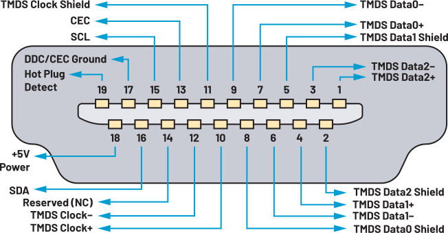
To ensure that the isolated link remains fully compliant with the HDMI specification, understanding the composition of the HDMI interface is crucial, as shown in Figure 1.
TMDS High-Speed Data and Clock Channels
HDMI uses four differential pairs (eight pins) for high-speed transmission.
- Three TMDS Data Channels (Data 0–2): Carry RGB video data, audio information, and auxiliary data.
- One TMDS Clock Channel: Provides the reference clock used by the sink to sample the data channels.
Data is encoded using 8b/10b coding to control transition density and DC balance.
Display Data Channel (DDC)
The DDC consists of two lines (SCL clock and SDA data). It is used by the source (for example, a PC) to read the display’s extended display identification data (EDID), which describes the supported resolutions and formats.
Consumer Electronics Control (CEC)
CEC is a single-wire bus that allows a single remote control to operate multiple HDMI connected devices, such as controlling a set top box via a television remote.
Hot Plug Detect (HPD)
The HPD line indicates the connection status of the sink. When a display is plugged in or powered on, HPD changes state to notify the source to initiate or reconfigure the video link.
Power and Ground
The HDMI connector provides a 5V supply that allows EDID to be read even if the display’s main power is off. Shield and ground connections ensure reference integrity and noise suppression.
Advanced Channels (HEAC: HDMI Ethernet and Audio Return Channel)
For cables and devices that support advanced features, certain pins may be repurposed for Ethernet data and audio return channel (ARC/eARC), enabling audio from the TV to be sent back to an AV receiver.
From an isolation perspective, the HDMI interface can be partitioned into:
- Four high-speed TMDS differential pairs (three data + one clock)
- Multiple low-speed control and status signals (DDC, CEC, HPD, HEAC, and 5V)
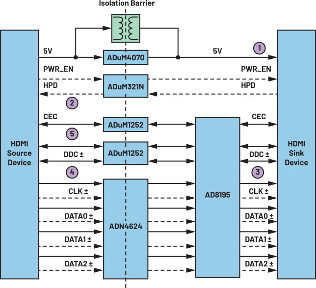
DDC and CEC are open drain, bidirectional low-speed signals. Their isolation must preserve I2C like behavior (for EDID reads and CEC arbitration) and voltage levels. Therefore, bidirectional digital isolators are required for these lines. HPD is a unidirectional status signal, for which a unidirectional isolator can be used.
A typical isolator selection strategy for an isolated HDMI design is as follows (see Figure 2).
- High-Speed TMDS Lanes: LVDS gigabit isolators such as the ADN4624 to carry the serialized high-speed data and clock.
- DDC and CEC: Bidirectional I2C/low-speed isolators capable of open drain behavior.
- HPD and Other Unidirectional Signals: Simple unidirectional digital isolators.
TMDS CML–to–LVDS Conversion Using AC Coupling and Bias Networks
A critical aspect of the design is the interface between the HDMI TMDS physical layer and the LVDS based isolator. TMDS employs current-mode logic (CML).
- CML uses a constant current source and external 50Ω pull up to 3.3V on each line to form the differential pair.
- The receiver expects a 100Ω differential load (two 50Ω terminations) referenced to 3.3V, with a typical differential swing of a few hundred millivolts.
In contrast, devices such as the ADN4624/ADN4654 are LVDS transceivers.
- They are voltage mode differential drivers/receivers with a characteristic 100Ω differential impedance.
- The acceptable common-mode voltage is typically around 1V to 1.5V, markedly lower than the 3.3V environment of TMDS.
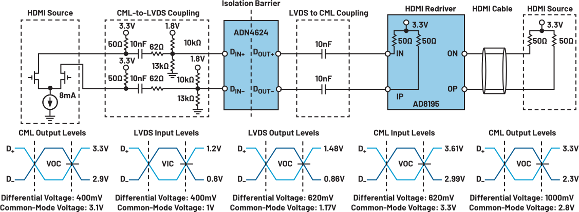
The key steps on the TMDS to LVDS side are as follows.
Step 1. Provide a proper TMDS termination for the HDMI source.
Each TMDS line is terminated with an effective 100Ω to 3.3V (implemented, for example, as two 50Ω resistors), providing the correct load and maintaining 100Ω differential impedance for the HDMI source driver.
Step 2. AC couple the differential pair.
Series capacitors (typically on the order of 10nF per line) block the DC common-mode voltage from the TMDS side while passing only the AC component of the differential signal.
Step 3. Re-establish a suitable LVDS common-mode voltage and termination.
On the LVDS input side of the isolator, a 200Ω differential termination is placed across the two input pins. In combination with any internal termination, this presents the correct effective load to the incoming signal.
Additionally, a bias network such as a resistor divider (for example, 10kΩ pull up to 3.3V and 10kΩ pull down to ground on each input line) sets the common-mode voltage to approximately 1V. The two lines, via this network, form the LVDS appropriate common-mode voltage while the AC coupled differential swings ride on top of it.
Using this approach, the original TMDS CML waveform is effectively translated into an LVDS compatible differential waveform without violating either side’s DC operating conditions. A symmetric structure can be applied after the isolation barrier to translate LVDS back into a TMDS compatible CML environment for the HDMI sink, as seen in Figure 3.
Maintaining HDMI Signal Integrity Through Isolation
Beyond protocol compatibility, the HDMI link must still pass the standard compliance tests after isolation. These include stringent limits on:
- Clock and data jitter
- Eye diagram mask margins
- Rise/fall times
- Inter-pair and intra-pair skew
Inserting a galvanic isolation stage can easily degrade these metrics through additive jitter, amplitude loss, and impedance discontinuities.
To preserve signal quality, the following techniques are recommended:
1. Loss and equalization management.
The cumulative loss from PCB traces, connectors, and isolation components should be minimized by controlling trace impedance, keeping differential pairs as short and direct as possible. For longer links or higher resolutions, HDMI buffers/equalizers such as the AD8195 can be used to compensate for high frequency loss and edge degradation.
2. Amplitude and termination control.
TMDS amplitude that is too low or exhibits excessive overshoot and undershoot often indicates issues in CML-to-LVDS biasing or termination, or excessive insertion loss from AC-coupling capacitors and electrostatic discharge (ESD) devices.
3. Skew management.
The four TMDS differential pairs (clock plus three data channels) must be tightly length matched, both within each pair (intra-pair skew) and across pairs (inter-pair skew). Multiple board transitions or long detours can lead to sampling errors at the sink.
4. Isolation gap and reference plane strategy.
To meet creepage and clearance requirements for MOPP/MOOP, ground and power planes must be physically separated at the isolation boundary. However, from a signal integrity perspective, each side of the isolation barrier should still maintain a solid reference plane up to the isolator pins.
Only the minimal region under and around the isolator package should be voided to create the required isolation distance. High-speed differential pairs should not run for long distances over plane voids or large slots, as this increases impedance discontinuities and electromagnetic interference (EMI).
5. Isolated power and EMI control.
Isolated power supplies must be designed with appropriate LC filtering and careful layout (short current loops, proper partitioning of split grounds) to prevent switching noise from coupling into the TMDS lines.
Extension to Other Applications
The methodology described above is not limited to HDMI. It can be extended to a range of high-speed, safety-critical applications; for example:
- Machine vision and industrial camera interfaces.
Interfaces such as Camera Link, GigE Vision, and custom LVDS streaming links share the same fundamental characteristics: high data rate differential pairs plus galvanic isolation requirements. The ADN46xx family of LVDS isolators can be adapted to these links using similar AC coupling and biasing schemes.
- Medical/industrial human-machine interface (HMI) and operating room displays.
Whether the video link is HDMI, DisplayPort, or a proprietary LVDS interface, any topology in which patient side imaging is transmitted to an operating room display or field camera feeds to a remote control room can benefit from the same isolation strategy. The design concerns for signal quality and safety are analogous to those of the HDMI use case.
Conclusion
The central challenge in isolating high-speed interfaces such as HDMI is to simultaneously preserve signal integrity at multi-gigabit per second data rates and satisfy stringent medical and industrial safety standards. Combined with high-speed digital isolators and medically rated isolated power modules, such designs can meet eye diagram, jitter, and MOPP/MOOP requirements.
At the PCB level, maintaining continuous reference planes on each side of the isolation barrier and limiting the interruption of these planes to the immediate vicinity of the isolator pins enables effective control of EMI and reflections. Overall, the described approach provides a robust and safe foundation for galvanically isolated video transmission in medical imaging systems such as endoscopes, as well as in broader industrial and machine vision applications.
References
“CN0571: Galvanically Isolated Full HD 1080p/60Hz HDMI PHY Using iCoupler® Isolation Technology.” Analog Devices, Inc., December 2024.
Patrick, Mark. “Emerging Power Standards in the Medical Industry.” SmartAuto Magazine, June 2018.
About the Authors
Cindy Chang is an applications engineer in the Central Applications Group at Analog Devices. She graduated with a bachelor’s degree in electrical engineering from University of California Los Angeles and joined ADI in July
Related to this Article
Products
RECOMMENDED FOR NEW DESIGNS
5.7 kV RMS/1.5 kV RMS, Quad-Channel LVDS 2.5 Gigabit Isolator (0 Reverse Channels)
RECOMMENDED FOR NEW DESIGNS
5 kV RMS/3.75 kV RMS, Dual LVDS Gigabit Isolator (0 Reverse Channels)
PRODUCTION
Isolated Switch Regulator with Integrated Feedback