

Overview
Design Resources
Design & Integration File
- Schematic
- Bill of Materials
- Assembly Files
- Gerber Files
- Allegro Layout File
Evaluation Hardware
Part Numbers with "Z" indicate RoHS Compliance. Boards checked are needed to evaluate this circuit.
- EVAL-ADPD188BI-ALGO Algorithm Package
- EVAL-ADPD188BI-DATA Dataset Package
- EVAL-CN0523-EBZ ($69.00) 5.8 GHz ISM Band Power Amplifier with Over Temperature Monitoring
Features & Benefits
- 5.8 GHz RF Power Amplifier
- 24 dB of Gain
- 50 Ohm matched SMA Input and Output Connectors
- Over Temperature Monitoring
- USB Powered
Documentation & Resources
-
EVAL-CN0523-EBZ User Guide (GitHub)4/16/2026
Circuit Function & Benefits
The International Telecommunication Union allocates the unlicensed 5.8 GHz industrial, scientific, and medical (ISM) radio frequency band for worldwide use. Advancements in wireless technologies and standards, as well as minimal regulatory compliance requirements, have made this frequency band popular for short range, wireless communication systems.
One popular application for the 5.8 GHz frequency band is Wi-Fi, where its 150 MHz channel bandwidth accommodates up to 24 non-overlapping Wi-Fi channels. While its transmission range is shorter than that of the 2.4 GHz frequency band, its higher per channel bandwidth makes it suitable for short distance, high data rate communication applications.
Other common uses can be found in software defined radio, wireless access points, public safety radio, wireless repeaters, femtocells, wireless broadband communication such as in 4G long term evolution (LTE) and worldwide interoperability for microwave access (WiMAX), and base transceiver station infrastructures. In any radio transmission application, a high gain amplifier is required to drive the antenna. This can be implemented in one or more stages depending on the application requirements, with higher output power values extending the range of the RF transmission. To achieve the optimal performance, several factors must be considered in the design, such as proper impedance matching, noise figure, frequency response, power management, and thermal management.
The circuit shown in Figure 1 is a two-stage, RF power amplifier optimized for transmit signal chains operating in the 5.8 GHz ISM band. The circuit has a gain of approximately 24 dB and an input return loss of approximately 11 dB at the center frequency. The RF input and output ports are designed with a 50 Ω impedance match, enabling direct connection between the circuit and standard 50 Ω systems.
To prevent overheating, a temperature monitoring switch circuit disables the RF amplifier when the user-defined temperature trip point is reached. This switch circuitry also automatically enables the amplifier when the temperature falls below the hysteresis set point.


Circuit Description
RF POWER AMPLIFIER
The CN0523 uses two HMC407 power amplifiers for its RF signal path. The HMC407 is a gallium arsenide (GaAs), indium gallium phosphide (InGaP), heterojunction bipolar transistor, monolithic microwave IC power amplifier operating between 5 GHz to 7 GHz for various applications such as U-NII and HiperLAN.
Figure 2 shows the HMC407 S-Parameter performance with a typical gain of 15 dB and return losses of more than 10 dB throughout its RF band of operation. With the two HMC407 cascaded together, the CN0523 achieves a total system gain of 24 dB.


The HMC407 has a 1 dB compression point (P1dB) of 25 dBm, a third-order intercept point (OIP3) of 40 dBm, a saturated output power of 28 dBm, and a noise figure of 5.5 dB.
Impedance Matching
The HMC407 does not require any external matching circuitry to operate. The RFIN and RFOUT pins are single-ended with an impedance of 50 Ω over the 5 GHz to 7 GHz frequency band, allowing the CN0523 to directly interface with a 50 Ω terminated system. Both RFIN and RFOUT have integrated DC-blocking capacitors that allow HMC407 amplifiers to be cascaded back-to-back without the need for external capacitors or an external matching network.
Figure 3 shows the basic configuration of HMC407 and the implementation of cascading two amplifiers.


BAND-PASS FILTER
The first stage amplifier output is filtered by a band-pass filter, which eliminates unwanted out-of-band amplification. The filter used has a pass band of 5.15 GHz to 5.95 GHz, with a return loss of 21 dB and an insertion loss of 0.7 dB at 5.8 GHz center frequency.
RF PERFORMANCE
The resulting S-Parameters, phase noise measurements, spurious- free dynamic range (SFDR), input and output power measurements, and stability measure of the CN0523 are shown in figures below.
At the center frequency of 5.8 GHz, the CN0523 achieves a gain of 24 dB with input and output return losses of greater than 10 dB. Figure 4 shows the S-Parameters across the operating frequency range.


Figure 5 shows the corresponding noise figure of approximately 6.5 dB over the entire frequency range.


Figure 6 shows the single sideband phase noise at 5.8 GHz, with offset values of approximately -114.91 dBc/Hz,-117.77 dBc/Hz, and -130.48 dBc/Hz at 10 kHz, 100 kHz, and 1 MHz, respectively.


Figure 7 presents the narrow-band single-tone RF output with an SFDR of 81 dB at an input power level of -2 dBm.


Figure 8 shows the output power (POUT) vs. input power (PIN) graph of the CN0523. The CN0523 has a saturation point of approximately +27 dBm and has an absolute maximum input power of +10 dBm. It is not recommended to operate the circuit above this input level as damage may incur.


The system is stable across the entire 5.8 GHz ISM frequency bandwidth with the Rollet's stability factor (k) being above 1 and the supplementary stability measure (B1) being above 0, as shown in Figure 9. This makes the CN0523 unconditionally stable for any combination of source and load impedance.


OVERTEMPERATURE MANAGEMENT
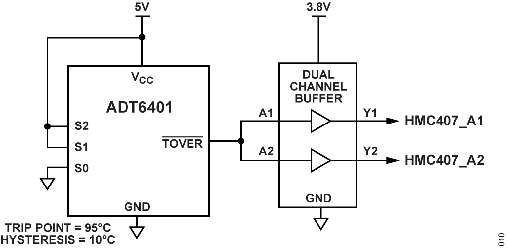
An overtemperature management feature is implemented on the CN0523 wherein the amplifiers are automatically disabled when the board temperature reaches a preset threshold. The CN0523 automatically returns to normal operation once the temperature falls below the hysteresis set point. This feature is done using the open-drain output (TOVER/TUNDER) function of the ADT6401 temperature switch, which monitors the temperature near the first stage HMC407 amplifier and compares it to a pin-programmable trip point.
Figure 10 shows the trip point monitoring circuitry using the ADT6401 temperature switch.


The states of Pins S0, S1, and S2 select the temperature trip point and hysteresis of the ADT6401. The available temperature trip point and hysteresis settings on the CN0523 are listed in Table 1.
| S0 | S1 | S2 | Temperature Trip Point | Hysteresis |
| 0 1 Float |
0 0 0 |
0 0 0 |
+45°C +55°C +65°C |
2°C 2°C 2°C |
| 0 1 Float |
1 1 1 |
0 0 0 |
+75°C +85°C +95°C |
2°C 2°C 2°C |
| 0 1 Float |
Float Float Float |
0 0 0 |
+105°C +115°C +55°C |
2°C 2°C 10°C |
| 0 1 Float 0 |
0 0 0 1 |
1 1 1 1 |
+65°C +75°C +85°C +95°C |
10°C 10°C 10°C 10°C |
By default, the CN0523 reference design uses a +95°C trip point and a +10°C hysteresis setting.
The HMC407 has an internal power-down capability that can be directly controlled using the ADT6401 output, as shown in Figure 11.

LAYOUT CONSIDERATIONS
The power amplifier produces a large amount of heat when in use; therefore, special attention must be given to the thermal dissipation. To ease the power dissipation, the CN0523 uses a 3-layer thick ground plane and multiple thermal vias were placed around and under the HMC407.
Figure 12 is a thermal camera image of the CN0523 operating with an input power of 0 dBm. At an ambient temperature of 17°C, the temperature at the surface of the HMC407 is approximately 80°C (a 63°C temperature rise). The ADT6401 sensor is located between the HMC407s and rises 47.7°C (above ambient) to 64.7°C, thus the HMC407's temperature rise is 1.321 times than that of the sensor.
Under these operating conditions, the ADT6401 reaches its trip point of 95°C at an ambient temperature of 47°C. With the HMC407 at 47°C ambient + 63°C rise, the trip point is at 110°C – well below the 150°C maximum die temperature. The trip point can be adjusted to suit other conditions, taking care to observe the 150°C maximum.


USB POWER MANAGEMENT
The CN0523 derives its power through a micro-USB adapter, which typically provides a 5 V, 1 A supply via the micro-USB port. The whole system requires an overall current of approximately 320 mA during normal operation.
The power requirements are provided using two supply voltages. The nominal 4.75 V to 5.25 V input from the USB port is boosted to 5.6 V, then post-regulated to 5.0 V and 3.3 V. Figure 13 shows the complete CN0523 power supply architecture.


The main +5 V power is regulated by an LT8364, a current-mode DC/DC converter with a 60 V, 4 A switch operating from a 2.8 V to 60 V input. With a unique single feedback pin architecture, this device is capable of boost, SEPIC or inverting configurations. Burst mode operation consumes as low as 9 μA quiescent current, which maintains high efficiency at very low output currents while keeping typical output ripple below 15 mV. Figure 14 shows the basic configuration needed to set the LT8364 for a 5.6 V output.


The output voltage is programmed with resistor divider from the output to the FBX pin of the LT8364. Equation 1 shows how to calculate a desired output voltage with the user-defined resistor values:

where:
VOUT is the desired output voltage in Volts.
R1, R2 are the user-defined resistor values.
For the required output voltage of +5 V, the equation results with R1 = 1 MΩ and R2 = 402 kΩ.
The two HMC407 amplifier stages also draw additional supply current at higher temperatures; but with a maximum output current of 1.7 A, the LT8364 is more than sufficient to handle the current requirements of the CN0523.
The ADM7171-5.0 LDO regulator is used to generate the 5 V, 220 mA power required by the two HMC407 and the ADT6401. It has an input range of 2.3 V to 6.5 V and is capable of driving a load of up to 1 A.
The ADM7171 LDO regulator is used to generate the 3.8 V, 15 mA power required by the buffer amplifier and power down pin (VPD) of the HMC407. This device has an input voltage range of 2.3 V to 6.5 V and an initial fixed output voltage of 3.3 V, but the fixed 3.3 V output of the ADM7171 can be maximized up to 3.8 V output using Equation 2:

where:
VOUT is the desired output voltage in Volts.
R1, R2 are the user-defined resistor values.
For the required output voltage of +3.8 V, the equation results with R1 = 1 kΩ and R2 = 6.49 kΩ which is shown in Figure 15.


Common Variations
The HMC451 can be used as an alternative power amplifier for the 5.8 GHz ISM band. Compared to HMC407, this device offers slightly higher gain (S21) and lower input return loss (S11) at the cost of having a lower 1 dB compression point, output return loss (S22), saturation power, and noise figure.
The ADT6402 can also be used as the temperature switch. This device is pin-compatible and shares the same specifications as the ADT6401, but has an active-low output and requires an inverting buffer.
Similar amplifier designs for transmitting signals in the 433.92 MHz, 915 MHz, and 2.45 GHz ISM bands are available. For more information, refer to the CN0551, CN0522, and CN0417 circuit notes, respectively.
Circuit Evaluation & Test
CIRCUIT EVALUATION AND TEST
This section covers the setup and procedure for the CN0523 circuit evaluation. For complete details, refer to the EVAL-CN0523-EBZ User Guide.
EQUIPMENT NEEDED
- CN0523 circuit evaluation board (EVAL-CN0523-EBZ)
- Signal generator (Rohde & Schwarz® SMA100B)
- Signal analyzer (Keysight® E5052B)
- Vector network analyzer (Keysight N5242A PNA-X)
- 5 V; ≥0.5 A AC/DC power adapter with micro-USB cable
- SMA cables
- 20 dB attenuator, which is optional for input protection of the signal analyzer.
SETUP AND TEST
Figure 16 shows the proper port connection of the EVAL-CN0523- EBZ to the vector network analyzer for S-Parameter and noise figure testing.


The procedure for measuring S-Parameters and noise figure are as follows:
- Set the desired measurement conditions of the vector network analyzer as follows:
- Set the frequency span from 5 GHz to 6 GHz.
- Set the frequency step size to 10 kHz.
- The power level must be less than or equal to -30 dBm.
- Perform a full 2-port calibration of the vector network analyzer
using a calibration kit.
Note: The RF input of the EVAL-CN0523-EBZ can be connected directly to a test port, so only one measurement cable is needed for the test setup.
- Connect the EVAL-CN0523-EBZ across the test ports of the vector network analyzer using the calibrated test setup.
- Power up the EVAL-CN0523-EBZ using the 5 V power adapter.
- Set the vector network analyzer to display the traces of the individual S-Parameters and the noise figure.
- Compare measurements to the expected values. At 5.8 GHz center frequency, the values for input and output return losses are approximately 11 dB and 15 dB, respectively. For the gain and noise figure readings, values should be approximately 24 dB and 6.5 dB, respectively.
Figure 17 shows the proper port connection of the EVAL-CN0523- EBZ to the signal analyzer and signal generator for phase noise and SFDR testing.


The procedure for measuring phase noise, SFDR, and POUT vs. PIN are as follows:
- Set the desired measurement conditions of the signal analyzer
as follows:
- For SFDR measurement, set the center frequency to 5.8 GHz, the frequency span to 5 GHz to 6 GHz.
- For phase noise measurement, set the center frequency to 5.8 GHz and the offset frequency range to 10 Hz to 1 GHz.
- Set the power level of the signal generator to -30 dBm with the center frequency set at 5.8 GHz.
- Connect the signal generator output to the RF input of the EVAL-CN0523-EBZ.
- Connect the RF output of the EVAL-CN0523-EBZ to the signal analyzer.
- Power up the EVAL-CN0523-EBZ using the 5 V power adapter.
- Execute a measurement run on the signal analyzer.
- Using the signal analyzer, get the phase noise value and verify if it is approximately -114.91 dBc/Hz at 10 kHz offset.
- . Run an SFDR test and compare the readings. The expected value is approximately 70 dBc.
- For POUT vs. PIN test, set the power level of the signal generator from -10 dBm to 0 dBm. Slowly ramp up the power level, then record the corresponding output power on the signal generator.