CN0294

Overview
Design Resources
Design & Integration File
- Schematic
- Bill of Materials
- Gerber Files
- PADS Files
- Assembly Drawing
Device Drivers
Software such as C code and/or FPGA code, used to communicate with component's digital interface.
ADF4350 IIO Wideband Synthesizer GitHub Linux Driver Source Code
Features & Benefits
- Integrated PLL and VCO
- Low Jitter fanout buffer
- LVPECL Outputs
Product Categories
Markets and Technologies
Parts Used
Documentation & Resources
-
UG-435: Evaluation Board for the ADF4351 Fractional-N PLL Frequency Synthesizer (Rev. 0)9/14/2015PDF1043 kB
-
UG-068: Setting Up the Evaluation Board for the ADCLK94811/16/2009PDF211 kB
-
MT-101: Decoupling Techniques2/14/2015PDF954 kB
-
MT-031: Grounding Data Converters and Solving the Mystery of "AGND" and "DGND"3/20/2009PDF144 kB
Circuit Function & Benefits
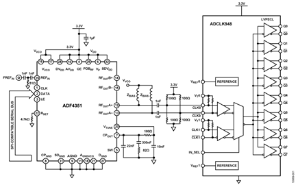
Many systems require low jitter multiple system clocks for mixed signal processing and timing. The circuit shown in Figure 1 interfaces the ADF4351 integrated phase-locked loop (PLL) and voltage-controlled oscillator (VCO) to the ADCLK948, which provides up to eight differential, low voltage, positive emitter coupled logic (LVPECL) outputs from one differential output of the ADF4351.


Modern digital systems often require many high quality clocks at logic levels that are different from the logic level of the clock source. Extra buffering may be required to guarantee accurate distribution to other circuit components without loss of integrity. The interface between the ADF4351 clock source ADCLK948 clock fanout buffer is described, and measurements show that the additive jitter associated with the clock fanout buffer is 75 fs rms.
Circuit Description
The ADF4351 is a wideband PLL and VCO consisting of three separate multiband VCOs. Each VCO covers a range of approximately 700 MHz (with some overlap between the frequencies of the VCO). This permits a fundamental VCO frequency range of between 2.2 GHz to 4.4 GHz. Frequencies lower than 2.2 GHz can be generated using internal dividers within the ADF4351.
For clock generation, the ADF4351 PLL and VCO must be enabled, and the desired output frequency must be programmed. The output frequency of the ADF4351 is available at the open-collector outputs at the RFOUT pins, which require a shunt inductor (or resistor), plus a dc blocking capacitor.
The ADCLK948 is a SiGe low jitter clock fanout buffer that is ideally suited for use with the ADF4351, because its maximum input frequency (4.5 GHz) is just above that of the ADF4351 (4.4 GHz). Broadband rms additive jitter is 75 fs.
It is necessary to add a dc common-mode bias level of 1.65 V to the CLK inputs of the ADCLK948 to mimic LVPECL logic levels. This is accomplished by the use of a resistor bias network. Omission of the dc bias circuit results in degraded signal integrity at the ADCLK948 outputs.
Common Variations
Other possible synthesizers with integrated VCOs are the ADF4350 fractional N (137 MHz to 4400 MHz) and the ADF4360 integer N series.
Other possible clock fanout buffers in the same family as the ADCLK948 are the ADCLK946 (6 LVPECL outputs), ADCLK950 (10 LVPECL outputs), and the ADCLK954 (12 LVPECL outputs).
Circuit Evaluation & Test
The circuit is evaluated using the EVAL-ADF4351EB1Z board for a clock source, with some minor modifications. The EVAL-ADF4351EB1Z board uses the standard ADF4351 programming software contained on the CD that accompanies the evaluation board. The ADCLK948/PCBZ is also required and can be used out of the box without modification.
Equipment Needed
The following equipment is needed:
- The EVAL-ADF4351EB1Z evaluation board kit with programming software
- The ADCLK948/PCBZ evaluation board
- A 3.3 V power supply
- Two cables to connect the 3.3 V supply to the ADCLK948/PCBZ
- Two short equal length SMA coaxial cables
- A high speed oscilloscope (2 GHz bandwidth) or an equivalent
- The R&S FSUP26 spectrum analyzer or an equivalent
- A PC with Windows® XP, Windows, Vista (32-bit), or Windows 7 (32-bit)
The SMA coaxial cable is required to connect the RFOUTA+ and RFOUTA− pins of the EVAL-ADF4351EB1Z to CLK0 and CLK0 pins of the ADCLK948/PCBZ.
Functional Block Diagram
For this experiment, the ADCLK948/PCBZ and the EVAL-ADF4351EB1Z are used. The boards are connected via a SMA cable to the ADCLK948/PCBZ, as shown in Figure 1.


Getting Started
The UG-435 user guide details the installation and use of the EVAL-ADF4351EB1Z evaluation software. UG-435 also contains board setup instructions and the board schematic, layout, and bill of materials. Necessary modifications to the board are the insertion of 100 Ω resistors after the dc blocking capacitor. The resistors are connected to 3.3 V and to GND. This should be done to both the RFOUTA+ and RFOUTA− pins to provide a common-mode voltage of 1.65 V (above the minimum required 1.5 V). This may necessitate scraping off the solder mask near these transmission lines.
The UG-068 user guide contains similar information relevant to the operation of the ADCLK948/PCBZ evaluation board.
Logic Level Measurement
In this example, the Rohde & Schwarz RTO1024 oscilloscope is used together with two RT-ZS30 active probes to accurately measure the high speed logic levels.
Install the ADF435x software to PC by doing the following:
- Connect the EVAL-ADF4351EB1Z to the PC, follow the hardware driver instructions as per UG-435.
- Program the ADF4351 PLL as per the screenshot of the ADF435x software (see Figure 3). In this example, an RF frequency of 1 GHz is chosen.
- Using two equal length short SMA cables, connect the RFOUTA+ and RFOUTA− SMA connectors from the EVAL-ADF4351EB1Z board to the CLK0/CLK0 SMA connectors of the ADCLK948/PCBZ board.
- Connect the differential output OUT2/OUT2 of the ADCLK948/PCBZ to the high speed oscilloscope. See Figure 4 for typical waveforms for a 1 GHz output.


Phase Noise and Jitter Measurement
- Repeat Step 1 to Step 4 from the Logic Level Measurement section.
- Terminate the unused CLK2 output of the ADCLK948/PCBZ with a 50 Ω load (see Figure 5).
- Connect the CLK2 output via a SMA cable to the signal source analyzer (see Figure 5).
- Measure the jitter performance of the signal.
Figure 6 shows the phase noise at the output of the ADF4351, and the rms jitter is 325.7 fs. Figure 7 shows the phase noise at the ADCLK948 output. The rms jitter is 330.4 fs.
The additive jitter of the ADCLK948 can be calculated as √(330.42 − 325.72) = 55.5 fs rms. The specified value from the ADCLK948 data sheet is 75 fs rms.


