Overview
Design Resources
Design & Integration File
- Schematic
- Bill of Materials
- PAD Files
- Assembly Drawing
Evaluation Hardware
Part Numbers with "Z" indicate RoHS Compliance. Boards checked are needed to evaluate this circuit.
- EVAL-CN0179-PMDZ ($41.96) Reference Design Board
- EVAL-SDP-CB1Z ($134.00) Eval Control Board
- SDP-PMD-IB1Z ($74.45) PMOD to SDP Interposer Board
Device Drivers
Software such as C code and/or FPGA code, used to communicate with component's digital interface.
Features & Benefits
- Low power 4-20 mA current loop
- 12-, 14-, or 16-bit digital control
- Use in programmable logic controllers
Product Categories
Markets and Technologies
Parts Used
Documentation & Resources
-
AN-345: Grounding for Low-and-High-Frequency Circuits2/14/2015PDF455 kB
-
AN-202: An IC Amplifier User’s Guide to Decoupling, Grounding, and Making Things Go Right for a Change (Rev. B)2/14/2015PDF76 K
-
AN-347: Shielding and Guarding2/14/2015PDF688 kB
-
CN0179 Software User Guide10/18/2018WIKI
-
The Data Conversion Handbook, 20051/2/2005
-
Op Amp Applications Handbook, 20051/2/2005
-
MT-015: Basic DAC Architectures II: Binary DACs (Rev. A)3/20/2009PDF100 kB
-
CN-0179: Less Than 200 μA, Low Power, 4 mA-to-20 mA, Process Control Current Loop1/11/2011PDF156 kB
Circuit Function & Benefits
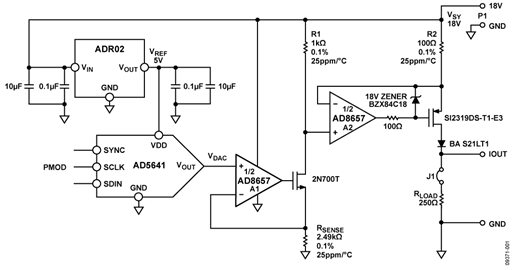
The circuit in Figure 1 is a 4 mA-to-20 mA current loop transmitter for communication between a process control system and its actuator. Besides being cost effective, this circuit offers the industry’s low power solution. The 4 mA-to-20 mA current loop has been used extensively in programmable logic controllers (PLCs) and distributed control systems (DCS’s), with digital or analog inputs and outputs. Current loop interfaces are usually preferred because they offer the most cost effective approach to long distance noise immune data transmission. The combination of the low power AD8657 dual op amp, AD5641DAC, and ADR02 reference allows more power budget for higher power devices, such as microcontrollers and digital isolators. The circuit output is 0 mA to 20 mA of current, and it operates on a single supply from 8 V to 18 V. The 4 mA to 20 mA range is usually mapped to represent the input control range from the DAC or micro-controller, while the output current range of 0 mA to 4 mA is often used to diagnose fault conditions.
The 14-bit, 5 V AD5641 requires 75 μA typical supply current. The AD8657 is a rail-to-rail input/output dual op amp and is one of the lowest power amplifiers currently available in the industry (22 μA per amplifier over the full supply voltage and input common-mode range) with high operating voltage of up to 18 V. The ADR02 ultracompact precision 5 V voltage reference requires only 650 μA. Together, these three devices consume a typical supply current of 747 μA.
The circuit has a 12-pin Pmod™ digital interface (Digilent specification).

Circuit Description
For industrial and process control modules, 4 mA-to-20 mA current loop transmitters are used as a means of communication between the control unit and the actuator. Located at the control unit, the 14-bit AD5641 DAC produces an output voltage, VDAC, between 0 V and 5 V as a function of the input code. The code is set via an SPI interface. The ideal relationship between the input code and output voltage is given by
where: VREF is the output of ADR02 and the power supply to the AD5641. D is the decimal equivalent of the binary code that is loaded to the AD5641.
The DAC output voltage sets the current flowing through the sense resistor, RSENSE, where
The current through RSENSE varies from 0 mA to 2 mA as a function of VDAC. This current develops a voltage across R1 and sets the voltage at the noninverting input of the AD8657 amplifier (A2). The A2 AD8657 closes the loop and brings the inverting input voltage to the same voltage as the noninverting input. Therefore, the current flowing through R1 is mirrored by a factor of 10 to R2. This is represented by Equation 3.
With VDAC ranging from 0 V to 5 V, the circuit generates a current output from 0 mA to 20 mA.
The AD5641 is a 14-bit DAC from the nanoDAC family and operates from the 5 V output voltage of the ADR02 reference. It has an on-chip precision output buffer that is capable of swinging from rail-to-rail (within 10 mV), thus allowing a high dynamic output range. With a supply voltage of 5 V, AD5641 consumes a typical 75 μA of supply current.
In addition, this circuit solution requires a rail-to-rail input amplifier. The AD8657 dual op amp is an excellent choice, with low power and rail-to-rail features. The op amp operates with a typical supply current of 22 μA/amplifier over the specified supply voltage and input common-mode voltage. It also offers excellent noise and bandwidth per unit of current. The AD8657 is one of the lowest power amplifiers that operate on supplies of up to 18 V.
The ADR02 is an ultracompact, precision 5 V voltage reference. With an 18 V input voltage, quiescent current is only 650 μA, typical. It has an initial accuracy of 0.06% (B-grade) and 10 μV p-p voltage noise. Connecting a 0.1 μF ceramic capacitor to the output is highly recommended to improve stability and filter out low level voltage noise. An additional 1 μF to 10 μF electrolytic, tantalum, or ceramic capacitor in parallel can improve load transient response. A 1 μF to 10 μF electrolytic, tantalum or ceramic capacitor can also be connected to the input to improve transient response in applications where the supply voltage may fluctuate. An additional 0.1 μF ceramic capacitor should be connected in parallel to reduce supply noise.
Bypass capacitors (not shown in Figure 1) are required. In this case, a 10 μF tantalum capacitor in parallel with a 0.1 μF ceramic capacitor should be placed on each power pin of each dual op amp. Details of proper decoupling techniques can be found in Tutorial MT-101.
Figure 2 shows the linearity of the system, that is the measured output current from the circuit DAC input code from 0 to full-scale.

Figure 3 shows the output current error plot in percent full-scale range. The overall worst-case error is approximately 0.35% measured over the output range between Code 256 and Code 16,128.

Figure 4 shows the calibrated output current error plot. Removing the gain and offset error from Figure 3, the accuracy is better than 0.05% measured over the output range between Code 256 and Code 16,128.

The data in Figure 3 and Figure 4 shows larger errors at zero and full-scale because the output buffer of the AD5641 DAC limits when its output is within 10 mV of either supply rail. The region between Code 0 and Code 255 as well as the region between Code 16,129 and Code 16,384 are therefore excluded from the linearity specifications. This corresponds to approximately 0 V to 80 mV and 4.92 V to 5.00 V at the DAC voltage output; and 0 mA to 0.32 mA and 19.68 mA to 20.00 mA referenced to the current output.
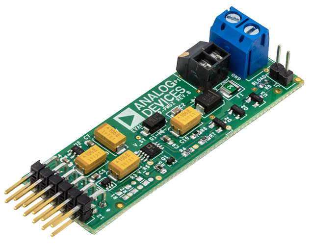
The test data was taken using the board shown in Figure 6. Complete documentation for the system can be found in the CN-0179 Design Support package.
Common Variations
For a 16-bit resolution solution, consider the AD5660 or AD5662, respectively. The 16 V CMOS ADA4665-2 op amp is another option to replace the AD8657. It lower cost and has lower voltage noise at the expense of a higher supply current.
When selecting amplifiers for this application, always ensure that the input common-mode voltage range and the supply voltage are not exceeded.
Circuit Evaluation & Test
This circuit uses the EVAL-CN0179-PMDZ circuit board, the EVAL-SDP-CB1Z system demonstration platform (SDP) evaluation board and the SDP-PMD-IB1Z, a Pmod interposer board for the EVAL-SDP-CB1Z. The SDP and the SDP-PMD-IB1Z boards have 120-pin mating connectors, allowing the quick setup and evaluation of the circuit’s performance. In order to evaluate the EVAL-CN0179-PMDZ board using the SDP-PMD-IB1Z and the SDP, the EVAL-CN0179-PMDZ is connected to the SDP-PMD-IB1Z by a standard 100 mil-spaced, 25 mil square, right angle 12 pin-Pmod header connector.
Information and details regarding how to use the evaluation software for data capturing and proper hardware installation can be found in the CN0179 Software User Guide.
Equipment Required
- PC with a USB port and Windows® XP, Windows® Vista (32-bit), or Windows® 7 (32-bit)
- EVAL-CN0179-PMDZ circuit evaluation board
- EVAL-SDP-CB1Z SDP evaluation board
- SDP-PMD-IB1Z
- CN0179 evaluation software
- Agilent E36311A dual dc power supply or equivalent
- Agilent 3458A multimeter or equivalent
- +6 V wall wart
- A GPIB-to-USB cable adapter (only required for capturing analog data from the output and transferring it to the PC)
Information and details regarding how to use the evaluation software for data capturing and proper hardware installation can be found in the CN0179 Software User Guide.
Test Setup and Measurements
The circuit was tested using the test setup in Figure 5. A photograph of the board is shown in Figure 6.
A jumper should not be connected to the J1 terminals when driving an external current loop. The jumper connects the internal 250 Ω load and should be used when making voltage measurements.


Figure 6. Photo of EVAL-CN0179-PMDZ Board


