CN0079

Overview
Features & Benefits
- Precision Digital to Analog Conversion
- Auto Zero Op-Amp Reduces Digital Switching Noise for 16-Bit DAC
Product Categories
Markets and Technologies
Parts Used
Circuit Function & Benefits
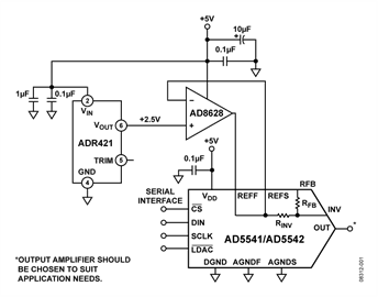
This circuit provides precision data conversion using the AD5542 voltage output DAC together with the ADR421BRZ voltage reference and the AD8628 auto-zero op amp as the reference buffer. The AD8628 reference buffer provide benefits previously found only in expensive auto-zeroing or chopper-stabilized amplifiers. Using Analog Devices, Inc., circuit topology, these zero-drift amplifiers combine low cost with high accuracy and low noise. No external capacitor is required, and the digital switching noise associated with most chopper-stabilized amplifiers is greatly reduced, thereby making this the optimum choice for reference buffering.
This circuit provides precision, low power, voltage output, digital-to-analog conversion. The AD5542 can be operated in either the buffered or unbuffered mode. The application and its requirements on settling time, input impedance, noise, etc., determine which mode of operation is best. The selection of the output buffer amplifier can be tailored to suit either dc precision or fast settling time. Where the DAC is required to drive a load less than 60 kΩ, an output buffer will be required. The output impedance of the DAC is constant and code independent, but to minimize gain errors the input impedance of the output amplifier should be as high as possible. The output amplifier should also have a 3 dB bandwidth of 1 MHz or greater. The output amplifier adds another time constant to the system, thereby increasing the settling time of the final output.
A higher 3 dB amplifier bandwidth results in a faster effective settling time of the combined DAC and amplifier. All devices in the circuit can be powered from a single +5 V supply. The input voltage range of the ADR421 reference is 4.5 V to 18 V.


Circuit Description
This circuit utilizes the AD5542 voltage output DAC, providing 16-bit, fully accurate performance. The DAC architecture of the AD5541/AD5542 is a segmented R-2R voltage mode DAC. With this type of configuration the output impedance is independent of digital code, while the input impedance seen by the reference is heavily code dependent. For this reason, the reference buffer choice is very important to account for the code-dependent reference current, which may lead to linearity errors if the DAC reference is not adequately buffered. The op amp offset voltage, offset error temperature coefficient, and noise are important criteria when selecting a reference buffer with precision voltage output DACs. Offset errors in the reference circuit cause gain errors on the DAC output. This circuit employs the AD8628 zero-drift, single-supply, rail-to-rail, input/output operational amplifier. With an offset voltage of 1 μV, drift of less than 0.005 μV/°C, and noise of 0.5 μV p-p (0.1 Hz to 10 Hz), the AD8628 is suited for applications where error sources need to be minimized. The output voltage is dependent on the reference voltage, as shown in the following equation:

where D is the decimal data-word loaded to the DAC register and N is the resolution of the DAC.
For a reference of 2.5 V, the equation is simplified to the following:

This gives a VOUT of 1.25 V for the midscale code and 2.5 V for the full-scale code.
The LSB size is 2.5 V/65,536, or 38.1 μV.
There is a common misconception that auto-zero amplifiers are not to be trusted because of intermodulation terms and unwanted harmonics filtering through to the output due to the internal switching action. Previous auto-zero amplifiers used either auto-zeroing or chopper stabilization techniques. Traditional auto-zeroing results in low noise energy at the auto-zeroing frequency at the expense of higher low frequency noise, due to aliasing of wideband noise into the auto-zeroed frequency band. Chopping results in less low frequency noise at the expense of larger noise energy at the chopping frequency. The AD8628 family uses both auto-zeroing and chopping in a patented "ping-pong" arrangement to obtain lower low frequency noise together with lower energy at the chopping and auto-zeroing frequencies, thereby maximizing the signal-to-noise ratio for the majority of applications without the need for additional filtering. The relatively high internal chopping frequency of 15 kHz simplifies filter requirements for a wide, useful, noise-free bandwidth in instrumentation and process control applications.
Measured results show that high accuracy, low noise performance with minimum high frequency intermodulation distortions transferred to the output is achievable using the AD8628 as a reference buffer in a high accuracy, high performance system.
Integral nonlinearity (INL) error is the deviation in LSBs of the actual DAC transfer function from an idealized transfer function. DNL error is the difference between an actual step size and the ideal value of 1 LSB. The circuit in Figure 1 provides 16-bit resolution with ±1 LSB INL error and ±1 LSB DNL error. Figure 2 and Figure 3 show the INL and DNL performance of the circuit.


The offset error and gain error were measured to be 10 μV and 170 μV, respectively. The gain error of ±5 LSBs and the zero-code error of ±1 LSB are within the specified 38 μV (with a 2.5 V reference) at ambient temperature.
Figure 4 shows a 0.1 Hz to 10 Hz noise plot for the circuit. The output of the DAC, VOUT, was connected to the input of a 0.1 Hz to 10 Hz bandwidth filter followed by an amplifier with a gain of 10,000. The voltage noise is captured on a scope. A very low peak-to-peak voltage of 57 mV is observed (5.7 μV with respect to the DAC output).


Figure 5 shows the DAC output using the spectrum analyzer sweeping from 100 Hz to 100 kHz. No significant IMD terms were observed, thus showing that auto-zero amplifiers such as the AD8628 used as reference buffers are excellent choices.


In any circuit where accuracy is important, it is helpful to carefully consider the power supply and ground return layout on the board. The printed circuit board (PCB) containing the circuit should have separate analog and digital sections. If the circuit is used in a system where other devices require an AGND-to-DGND connection, the connection should be made at one point only. This ground point should be as close as possible to the AD5542. The power supply to the AD5542 should be bypassed with 10 μF and 0.1 μF capacitors. The capacitors should be as physically close as possible to the device, with the 0.1 μF capacitor ideally right up against the device. The 10 μF capacitors are the tantalum bead type. It is important that the 0.1 μF capacitor have low effective series resistance (ESR) and low effective series inductance (ESL), as is typical of common ceramic types of capacitors. This 0.1 μF capacitor provides a low impedance path to ground for high frequencies caused by transient currents due to internal logic switching. The power supply line should have as large a trace as possible to provide a low impedance path and reduce glitch effects on the supply line. Clocks and other fast switching digital signals should be shielded from other parts of the board by digital ground.
The circuit must be constructed on a multilayer PC board with a large area ground plane. Proper layout, grounding, and decoupling techniques must be used to achieve optimum performance (see Tutorial MT-031, Grounding Data Converters and Solving the Mystery of AGND and DGND and Tutorial MT-101, Decoupling Techniques).
Common Variations
The AD8538 is another excellent auto-zero op amp candidate to be used for buffering the reference in this circuit. It provides a low offset voltage and ultralow bias current. The 2.5 V output ADR421 can be replaced by either the ADR423 or the ADR434, which are low noise references available from the same reference family as the ADR421 and provide 3 V and 4.096 V, respectively. The ADR441 and the ADR431 ultralow noise references are suitable substitutes that provide 2.5 V, also. Note that the size of the reference input voltage is restricted by the rail-to-rail output voltage capability of the operational amplifier selected.
There is no output buffer used in this circuit because output buffer performance can be optimized for speed or dc precision, depending on the system bandwidth and application need. The AD5661 would be an excellent choice for an output buffer. This is a single-supply, 5 V to 16 V amplifier that uses Analog Devices’ patented DigiTrim™ technique to achieve low offset voltage. It features low input bias current and wide signal bandwidth. The AD8605 or the AD8655 would also be excellent options.