Overview
Design Resources
Design & Integration File
- Schematic
- Bill of Materials
- Gerber Files
- PADS Files
- Assembly Drawing
Evaluation Hardware
Part Numbers with "Z" indicate RoHS Compliance. Boards checked are needed to evaluate this circuit.
- EVAL-CFTL-6V-PWRZ ($23.01) Wall Power Supply
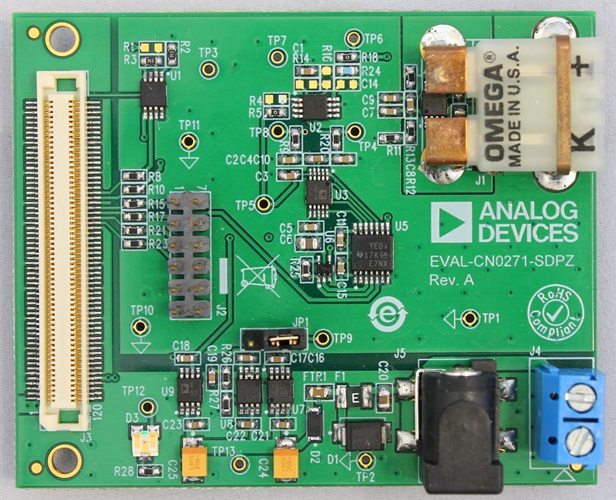
- EVAL-CN0271-SDPZ ($108.28) K-Type Thermocouple Measurement System with Integrated Cold Junction Compensation
- EVAL-SDP-CB1Z ($134.00) Eval Control Board
Device Drivers
Software such as C code and/or FPGA code, used to communicate with component's digital interface.
Features & Benefits
- Typical temperature range of -200 C to +1200 C
- K-type thermocouple measurement system
- 16-bit ADC, Low temperature drift
- Integrated cold junction compensation
Product Categories
Markets and Technologies
Parts Used
Documentation & Resources
-
CN-0271 Software User Guide10/22/2018WIKI
-
MT-068: Difference and Current Sense Amplifiers5/13/2016PDF244 kB
-
MT-101: Decoupling Techniques2/14/2015PDF954 kB
-
MT-035: Op Amp Inputs, Outputs, Single-Supply, and Rail-to-Rail Issues2/14/2015PDF115 kB
-
MT-031: Grounding Data Converters and Solving the Mystery of "AGND" and "DGND"3/20/2009PDF144 kB
-
MT-036: Op Amp Output Phase-Reversal and Input Over-Voltage Protection12/11/2008PDF653 kB
Circuit Function & Benefits
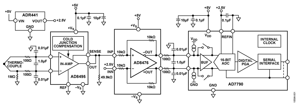
The circuit shown in Figure 1 is a complete thermocouple signal conditioning circuit with cold junction compensation followed by a 16-bit sigma-delta (Σ-Δ) analog-to-digital converter (ADC). The AD8495 thermocouple amplifier provides a simple, low cost solution for measuring K type thermocouple temperatures, including cold junction compensation.
A fixed gain instrumentation amplifier in the AD8495 amplifies the small thermocouple voltage to provide a 5 mV/°C output. The high common-mode rejection of the amplifier blocks commonmode noise that the long thermocouple leads can pick up. For additional protection, the high impedance inputs of the amplifier make it easy to add extra filtering.
The AD8476 differential amplifier provides the correct signal levels and common-mode voltage to drive the AD7790 16-bit, Σ-Δ ADC.
The circuit provides a compact low cost solution for thermocouple signal conditioning and high resolution analog-to-digital conversion.
Circuit Description
The thermocouple is a simple, widely used component for measuring temperature. It consists of a junction of two dissimilar metals. These metals are connected at one end to form the measurement junction, also called the hot junction. The other end of the thermocouple is connected to the metal lines that lead to the measurement electronics. This connection forms a second junction: the reference junction, also called the cold junction. To derive the temperature at the measurement junction (TMJ), the user must know the differential voltage created by the thermocouple. The user must also know the error voltage generated by the temperature at the reference junction (TRJ). Compensating for the reference junction error voltage is called cold junction compensation. The electronics must compensate for any changes in temperature at the reference (cold) junction so that the output voltage is an accurate representation of the hot junction measurement.
The circuit uses the AD8495 thermocouple amplifier on a single 5 V supply. The output voltage of the AD8495 is calibrated for 5 mV/°C. On a single 5 V supply, the output is linear between approximately 75 mV and 4.75 V, corresponding to a temperature range of 15°C to 950°C. The output of the AD8495 drives the noninverting input of the AD8476 unity-gain differential amplifier, which converts the single-ended input to differential outputs for driving the AD7790 16-bit, Σ-Δ ADC.
A low-pass differential and common-mode filter before the input of the AD8495 prevents RF signals, which, if allowed to reach the AD8495, can be rectified and appear as temperature fluctuations. The two 100 Ω resistors and the 1 μF capacitor form a differential filter with a cutoff frequency of 800 Hz. The two 0.01 μF capacitors form common-mode filters with a cutoff frequency of 160 kHz. A similar filter is used at the output of the AD8476 differential amplifier before the signal is applied to the AD7790 ADC.
The AD8495 inputs are protected from input voltage excursions up to 25 V from the opposite supply rail. For example, in this circuit, with a 5 V positive supply rail and the negative supply rail tied to GND, the part can safely withstand voltages at the inputs from -20 V to +25 V. Voltages at the reference and sense pins should not go beyond 0.3 V of the supply rails. This feature is of particular importance in applications with power supply sequencing issues that can cause the signal source to be active before the supplies to the amplifier are applied.
The theoretical resolution of the system can be calculated from the bandwidth, voltage noise density, and gain of the AD8495. The peak-to-peak (noise free code) resolution in bits is


The AD8476 is a very low power, fully differential precision amplifier with integrated thin film, laser trimmed 10 kΩ gain resistors for unity gain. It is an ideal choice for this application because it presents a relatively high impedance load to the AD8495.
The AD7790 is a low power, complete analog front end for low frequency measurement applications. It contains a low noise, 16-bit, Σ-Δ ADC with one differential input that can be buffered or unbuffered.
Test Results
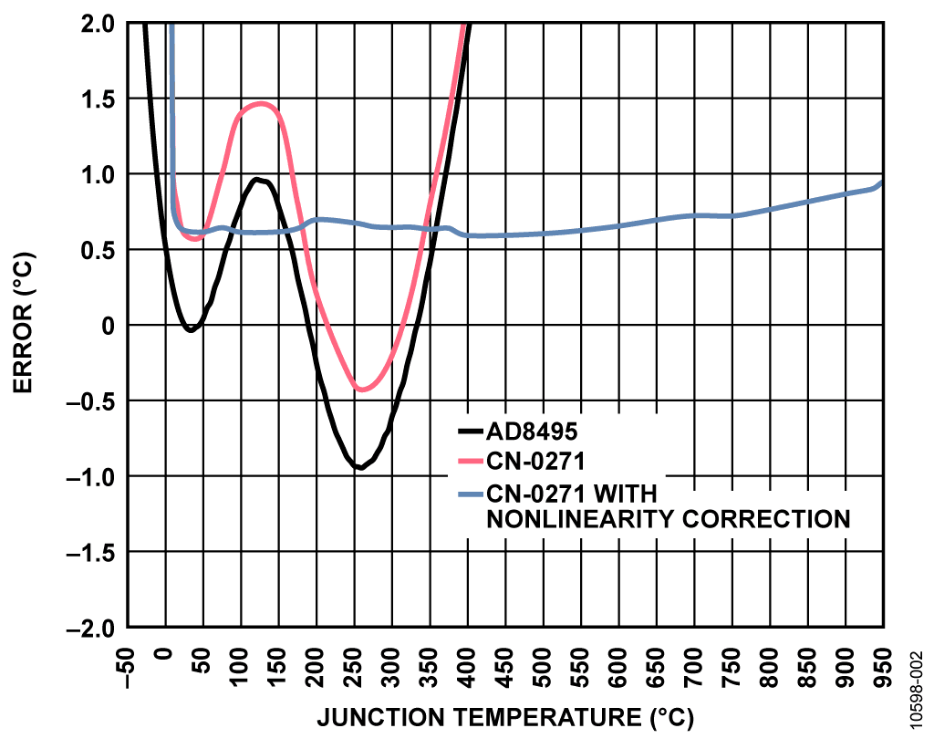
An important measure of the performance of the circuit is the amount of linearity error. The AD8495 output is accurate to within 2°C from -25°C to +400°C. To achieve even greater accuracy when operating at or outside of this range, a linearity correction algorithm must be implemented in software. The CN-0271 evaluation software uses NIST thermoelectric voltage lookup tables to achieve an output error within 1°C from 15°C to 950°C.
Figure 2 compares the performance of the AD8495 with the CN-0271 system, and the result of applying the linearization correction to the ADC output. For details on how the algorithm was implemented in the software, see the AN-1087 Application Note, Thermocouple Linearization When Using the AD8494/AD8495/AD8496/AD8497.
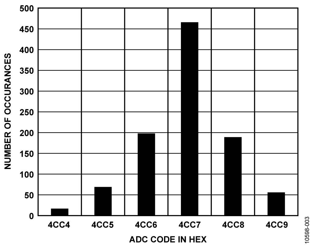
The noise performance of the system is also important to the accuracy of the circuit. Figure 3 shows a histogram of 1,000 measurement samples. This data was taken with the CN0271 evaluation board connected to the EVAL-SDP-CB1Z System Demonstration Platform (SDP-B) evaluation board. Details of the setup are described in the Circuit Evaluation and Test section.
The measured peak-to-peak noise is approximately 6 LSBs (1 LSB = 4.9 V ÷ 65536 = 74.8 μV), corresponding to 0.449 mV p-p and 13.4 bits of noise free resolution.

This shows that the converter does not decrease the noise free resolution because the measured resolution of a fixed thermocouple input voltage results in approximately the same number of noise free bits as predicted by the theoretical output noise of the AD8495.
A complete design support package for this circuit note can be found at www.analog.com/CN0271-DesignSupport.
Common Variations
To measure negative temperatures, apply a voltage at the reference pin to offset the output voltage at 0°C. The output voltage of the AD8495 is
VOUT = (TMJ × 5 mV/°C) + VREF
The complete K type thermocouple range of −200°C to +1250°C can be measured by modifying the circuit to run on dual supplies. When operating the AD8495 on a single supply, measurement of temperatures less than ambient become nonlinear because the output starts to saturate close to the supply rail. To maintain accuracy at lower temperatures, use dual supplies or level-shift the output by applying the appropriate offset voltage to the reference pin.
The AD8494 is calibrated for J type thermocouples. Both the AD8494 and AD8495 are optimized for reference junctions between 0°C and 50°C.
The AD8496 (J type) and AD8497 (K type) are optimized for reference junctions between 25°C and 100°C.
The circuit is proven to work with good stability and accuracy.
Circuit Evaluation & Test
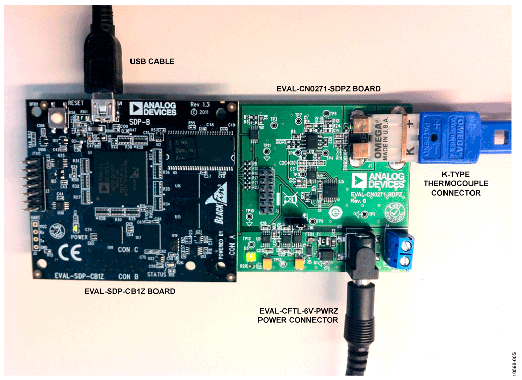
This circuit uses the EVAL-CN0271-SDPZ circuit board and the System Demonstration Platform (SDP-B) controller board (EVAL-SDP-CB1Z). The two boards have 120-pin mating connectors, allowing for the quick setup and evaluation of the performance of the circuit. The EVAL-CN0271-SDPZcontains the circuit to be evaluated, as described in this note, and the SDP-B controller board is used with the CN-0271 evaluation software to capture the data from the EVAL-CN0271-SDPZ circuit board.
Equipment Needed
The following equipment is needed:
- A PC with a USB port and Windows® XP or Windows Vista® (32-bit), or Windows® 7 (32-bit)
- The EVAL-CN0271-SDPZ circuit evaluation board
- The SDP-B controller board ( EVAL-SDP-CB1Z) or the SDP-S controller board (EVAL-SDP-CS1Z)
- The CN-0271 SDP evaluation software
- The 6 V power supply (EVAL-CFTL-6V-PWRZ) or equivalent dc power supply
Getting Started
Load the evaluation software by placing the CN-0271 evaluation software CD in the CD drive of the PC. Using My Computer, locate the drive that contains the evaluation software.
Functional Block Diagram
See Figure 1 of this circuit note for the circuit block diagram and the EVAL-CN0271-SDPZ-SCH-RevA.pdf file for the circuit schematics. This file is contained in the CN0271 Design Support Package.
Setup
Connect the 120-pin connector on the EVAL-CN0271-SDPZ circuit board to the CON A connector on the SDP-B controller board ( EVAL-SDP-CB1Z). Use nylon hardware to firmly secure the two boards, using the holes provided at the ends of the 120-pin connectors.
With power to the supply off, connect the EVAL-CFTL-6V-PWRZ plug to the barrel connector designated by J5 on the board. If this is unavailable, connect the +6V and GND pins to the provided two pin screw of J4 on the board. Also, connect the USB cable supplied with the SDP-B board to the USB port on the PC. Then, connect a K type thermocouple connector to J1 on the board and the other end to the test equipment.
With power to the supply off, connect the EVAL-CFTL-6V-PWRZ plug to the barrel connector designated by J5 on the board. If this is unavailable, connect the +6V and GND pins to the provided two pin screw of J4 on the board. Also, connect the USB cable supplied with the SDP-B board to the USB port on the PC.
Then, connect a K type thermocouple connector to J1 on the board and the other end to the test equipment.
Test
Launch the evaluation software and connect the USB cable from the PC to the mini-USB connector on the SDP-B board. Once USB communications are established, the SDP-B board can now be used to send, receive, and capture serial data from the EVAL-CN0271-SDPZ board.
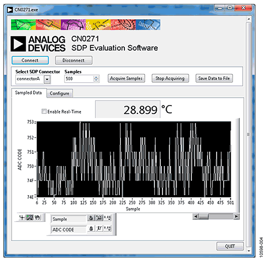
Figure 4 shows a screenshot of the CN-0271 SDP-B evaluation software interface, and Figure 5 shows a photo of the EVAL-CN0271-SDPZ evaluation board and the SDP-B board. Information regarding the SDP-B board can be found in the UG-277 user guide.
