Overview
Design Resources
Design & Integration File
- Schematic
- Bill of Materials
- Gerber Files
- PADS Files
- Assembly Drawing
Evaluation Hardware
Part Numbers with "Z" indicate RoHS Compliance. Boards checked are needed to evaluate this circuit.
- EVAL-CFTL-6V-PWRZ ($23.01) Wall Power Supply for Eval Board
- EVAL-CN0216-ARDZ ($54.14) Arduino Form Factor Weigh Scale Design
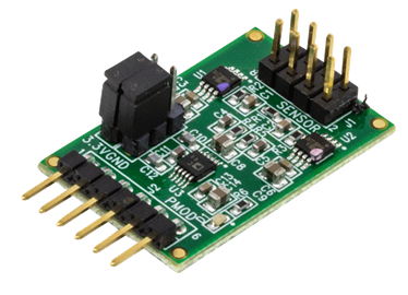
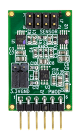
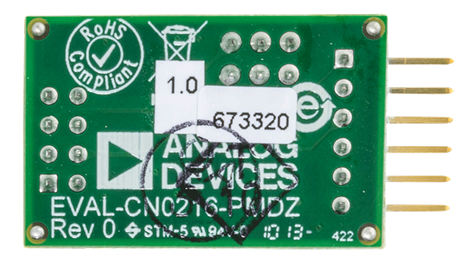
- EVAL-CN0216-PMDZ ($49.22) PMOD Form Factor Weigh Scale Design
- EVAL-CN0216-SDPZ ($81.21) Precision Weigh Scale Design Using the AD7791 24-Bit Sigma-Delta ADC with External ADA4528-1 Zero-Drift Amplifiers
- EVAL-SDP-CB1Z ($134.00) Eval Control Board SDP
Device Drivers
Software such as C code and/or FPGA code, used to communicate with component's digital interface.
AD778x Linux GitHub Driver Source Code
Features & Benefits
- High gain of 400 using zero drift amps
- Typical connection to weigh scales with low output signals
- Performance metrics maintained through 120 Hz
- Precision weigh scale application circuit
- Low power and low noise
Product Categories
Markets and Technologies
Parts Used
Documentation & Resources
-
CN0216 Software User Guide10/18/2018WIKI
-
MT-101: Decoupling Techniques2/14/2015PDF954 kB
-
MT-023: ADC Architectures IV: Sigma-Delta ADC Advanced Concepts and Applications2/14/2015PDF936 kB
-
MT-022: ADC Architectures III: Sigma-Delta ADC Basics2/14/2015PDF289 kB
-
MT-031: Grounding Data Converters and Solving the Mystery of "AGND" and "DGND"3/20/2009PDF144 kB
-
MT-004: The Good, the Bad, and the Ugly Aspects of ADC Input Noise - Is No Noise Good Noise?3/4/2009PDF342 kB
-
MT-063: Basic Three Op Amp In-Amp Configuration2/3/2009PDF68 kB
Circuit Function & Benefits
The circuit in Figure 1 is a precision weigh scale signal conditioning system. It uses the AD7791, a low power buffered 24-bit sigma-delta ADC along with two external ADA4528-1 zero-drift amplifiers. This solution allows for high dc gain with a single supply.
Ultralow noise, low offset voltage, and low drift amplifiers are used at the front end for amplification of the low-level signal from the load cell. The circuit yields 15.3 bit noise-free code resolution for a load cell with a full-scale output of 10 mV.
This circuit allows great flexibility in designing a custom low-level signal conditioning front end that gives the user the ability to easily optimize the overall transfer function of the combined sensor-amplifier-converter circuit. The AD7791 maintains good performance over the complete output data range, from 9.5 Hz to 120 Hz, which allows it to be used in weigh scale applications that operate at various low speeds.

Circuit Description
Figure 2 shows the actual test setup. For testing purposes, a 6-wire Tedea-Huntleigh 505H-0002-F070 load cell is used.
Current flowing through a PCB trace produces an IR voltage drop, and with longer traces, this voltage drop can be several millivolts or more, introducing a considerable error. A 1 inch long, 0.005 inch wide trace of 1 oz copper has a resistance of approximately 100 mΩ at room temperature. With a load current of 10 mA, this can introduce a 1 mV error.
A 6-wire load cell has two sense pins, in addition to the excitation, ground, and two output connections. The sense pins are connected to the high side (excitation pin) and low side (ground pin) of the Wheatstone bridge. The voltage developed across the bridge can be accurately measured regardless of the voltage drop due to wire resistance. In addition, the AD7791 accepts differential analog inputs and a differential reference as well. These two sense pins are connected to the AD7791 reference inputs to create a ratiometric configuration that is immune to low frequency changes in the power supply excitation voltage. The ratiometric connection eliminates the need for a precision voltage reference.
Unlike a 6-wire load cell, a 4-wire load cell does not have sense pins, and the ADC differential reference pins are connected directly to the excitation voltage and ground. With this connection, there exists a voltage difference between the excitation pin and the reference pin on the ADC due to wire resistance. There will also be a voltage difference on the low side (ground) due to wire resistance. The system will not be completely ratiometric.
The Tedea-Huntleigh 2 kg load cell has a sensitivity of 2 mV/V and a full-scale output of 10 mV when the excitation voltage is 5 V. A load cell also has an offset, or TARE, associated with it. In addition, the load cell also has a gain error. Some customers use a DAC to remove or null the TARE. When the AD7791 uses a 5 V reference, its differential analog input range is equal to ±5 V, or 10 V p-p. The circuit in Figure 1 amplifies the load cell output by a factor of 375 (1 + 2R1/RG), so the full-scale input range referred to the load cell output is 10 V/375 = 27 mV p-p. This extra range relative to the 10 mV p-p load cell full-scale signal is beneficial as it ensures that the offset and gain error of the load cell do not overload the ADC’s front end.
The low-level amplitude signal from the load cell is amplified by two ADA4528-1 zero-drift amplifiers. A zero-drift amplifier, as the name suggests, has a close to zero offset voltage drift. The amplifier continuously self-corrects for any dc errors, making it as accurate as possible. Besides having low offset voltage and drift, a zero-drift amplifier also exhibits no 1/f noise. This important feature allows precision weigh scale measurement at dc or low frequency.
The two ADA4528-1 op amps are configured as the first stage of a three op amp instrumentation amplifier. A third op amp connected as a difference amplifier would normally be used for the second stage, but in the circuit of Figure 1, the differential input of the AD7791 performs this function.
The gain is equal to 1 + 2R1/RG. Capacitors C1 and C2 are placed in the feedback loops of the op amps and form 4.3 Hz cutoff frequency low-pass filters with R1 and R2. This limits the amount of noise entering the sigma-delta ADC. C5 in conjunction with R3 and R4 form a differential filter with a cutoff frequency of 8 Hz, which further limits the noise. C3 and C4 in conjunction with R3 and R4 form common-mode filters with a cutoff frequency of 159 Hz.
The ADP3301 low noise regulator powers the AD7791, ADA4528-1, and the load cell. In addition to decoupling capacitors, a noise reduction capacitor is placed on the regulator output as recommended in the ADP3301 data sheet. It is essential that the regulator is low noise, because any noise on the power supply or ground plane introduces noise into the system and degrades the circuit performance.

The 24-bit sigma-delta ADC AD7791 converts the amplified signal from the load cell. The AD7791 is configured to operate in the buffered mode to accommodate the impedance of the R-C filter network on the analog input pins.
Figure 3 shows the AD7791’s rms noise for different output data rates. This plot shows that the rms noise increases as the output data rate increases. However, the device maintains good noise performance over the complete range of output data rates.

The AD7791 rms noise of 1.1 μV for a 9.5 Hz output data rate and a reference of 2.5 V yields the following number of noise-free counts:

where the factor of 6.6 converts the rms voltage into a peak-to-peak voltage.
The corresponding noise-free code resolution is, therefore:

Note that this represents the performance of the AD7791 without the load cell or the input amplifier connected.
The ADA4528-1 has 5.9 nV/√Hz of voltage noise density and, therefore, the input amplifiers and resistors will add noise to the system. In addition, the load cell itself will add noise.
In the circuit of Figure 1, a 5 V reference is used, therefore, the peak-to-peak input range is 10 V. The LSB is, therefore, equal to

The 10 mV p-p full-scale signal from the load cell produces a 3.75 V p-p signal into the ADC, which is approximately 38% of the ADC range.
Seven sets of 500 samples each were taken with the load cell connected (no load). The peak-to-peak code spread for each sample set was calculated, and the seven values averaged to yield a code spread of 159 counts. This corresponds to 159 × 0.596 μV = 94.8 μV p-p noise based on a full-scale input to the ADC of 3.75 V p-p.
Therefore, the number of noise-free counts is

Therefore, the corresponding noise-free code resolution of the total system is:

Figure 4 shows a plot of the ADC codes for 500 samples (52.6 sec for 9.5 Hz data rate). Note that the peak-to-peak spread is about 160 codes.

Figure 5 shows the same data presented in a histogram. Figure 4 and Figure 5 show the actual (raw) conversions read back from the AD7791. In practice, a digital post filter is typically used in a weigh scale system. The additional averaging that is performed in the post filter will further improve the number of noise-free counts at the expense of a reduced data rate.
The resolution of the system in grams can be calculated by

As with any high accuracy circuit, proper layout, grounding, and decoupling techniques must be employed. See Tutorial MT-031, Grounding Data Converters and Solving the Mystery of AGND and DGND and Tutorial MT-101, Decoupling Techniques for more details. A complete design support package for this circuit note can be found at www.analog.com/CN0216-DesignSupport.

Common Variations
Other ADCs and circuits suitable for weigh scale applications are discussed in CN-0102 (AD7190), CN-0107 (AD7780), CN-0108 (AD7781), CN-0118 (AD7191), CN-0119 (AD7192), and CN-0155 (AD7195).
The AD7171 is a 16-bit sigma-delta ADC.
For a lower power consumption solution, use the ADA4051-2. The ADA4051-2 is a dual micropower, zero-drift amplifier with only 20 μA of supply current per amplifier.
Circuit Evaluation & Test
This circuit uses the EVAL-CN0216-SDPZ circuit board and the EVAL-SDP-CB1Z system demonstration platform (SDP) evaluation board. The two boards have 120-pin mating connectors, allowing for the quick setup and evaluation of the circuit’s performance. The EVAL-CN0216-SDPZ board contains the circuit to be evaluated, as described in this note, and the SDP evaluation board is used with the CN-0216 evaluation software to capture the data from the EVAL-CN0216-SDPZ circuit board.
Equipment Needed
- PC with a USB port and Windows XP or Windows Vista (32-bit), or Windows 7 (32-bit)
- EVAL-CN0216-SDPZ circuit evaluation board
- EVAL-SDP-CB1Z SDP evaluation board
- CN0216 evaluation software
- Tedea-Huntleigh 505H-0002-F070 load cell or equivalent
- Power supply: +6 V, or +6 V “wall wart”
Getting Started
Load the evaluation software by placing the CN0216 Evaluation Software disc in the CD drive of the PC. Using My Computer, locate the drive that contains the evaluation software disc and open the Readme file. Follow the instructions contained in the Readme file for installing and using the evaluation software.
Functional Block Diagram
See Figure 1 of this circuit note for the circuit block diagram, and the PDF file “EVAL-CN0216-SDPZ-SCH” for the circuit schematics. This file is contained in the CN0216 Design Support Package.
Setup
Connect the 120-pin connector on the EVAL-CN0216-SDPZ circuit board to the connector marked “CON A” on the EVAL-SDP-CB1Z evaluation (SDP) board. Nylon hardware should be used to firmly secure the two boards, using the holes provided at the ends of the 120-pin connectors. Connect the load cell the EVAL-CN0216-SDPZ board.
With power to the supply off, connect a +6 V power supply to the pins marked “+6 V” and “GND” on the board. If available, a +6 V "wall wart" can be connected to the barrel jack connector on the board and used in place of the +6 V power supply. Connect the USB cable supplied with the SDP board to the USB port on the PC. Note: Do not connect the USB cable to the mini USB connector on the SDP board at this time.
Test
Apply power to the +6 V supply (or “wall wart”) connected to EVAL-CN0216-SDPZ circuit board. Launch the evaluation software and connect the USB cable from the PC to the USB mini-connector on the SDP board. The software will be able to communicate to the SDP board if the Analog Devices System Development Platform driver is listed in the Device Manager.
Once USB communications are established, the SDP board can now be used to send, receive, and capture serial data from the EVAL-CN0216-SDPZ board.
Information and details regarding how to use the evaluation software for data capture can be found in the CN0216 Evaluation Software Readme file.
Information regarding the SDP board can be found in the SDP User Guide.
Analyzing the Data
At least 500 samples of the ADC output data should be taken. Once the sample set is exported to a spreadsheet program, such as Excel, the samples can be analyzed. The standard deviation of the samples is approximately equal to the rms noise, assuming a Gaussian noise distribution. The peak-to-peak noise is approximately equal to the rms value multiplied by 6.6.
The peak-to-peak noise can also be taken directly from the sample set by simply taking the difference between the largest and smallest sample. In practice, the results obtained using this method were approximately the same as the value obtained by multiplying the rms value by 6.6.
The values obtained from the sample set are in LSBs, so they must be converted into voltage, where 1 LSB = 0.596 μV for a 5 V reference.
If desired, the results of several sample sets can be averaged to get a more accurate measurement.
Noise-free code resolution is calculated from the peak-to-peak noise as described previously in this circuit note.


