Overview
Design Resources
Design & Integration File
- Schematic
- Bill of Materials
- Gerber Files
- PAD Files
- Assembly Drawing
Evaluation Hardware
Part Numbers with "Z" indicate RoHS Compliance. Boards checked are needed to evaluate this circuit.
- EVAL-AD7781EBZ ($82.26) Weigh Scale Design Using the AD7781 20-Bit Sigma-Delta ADC with Internal PGA
Device Drivers
Software such as C code and/or FPGA code, used to communicate with component's digital interface.
AD7780 IIO Low Power Sigma-Delta ADC GitHub Linux Driver Source Code
Features & Benefits
- 20-bit Weigh scale application circuit
- Integrated PGA allows for wide array of weigh scales
- Low power and low cost
- Typically used in portable weigh scale applications
Product Categories
Markets and Technologies
Parts Used
Documentation & Resources
-
MT-023: ADC Architectures IV: Sigma-Delta ADC Advanced Concepts and Applications2/14/2015PDF936 kB
-
MT-022: ADC Architectures III: Sigma-Delta ADC Basics2/14/2015PDF289 kB
-
MT-004: The Good, the Bad, and the Ugly Aspects of ADC Input Noise - Is No Noise Good Noise?3/4/2009PDF342 kB
Circuit Function & Benefits
This circuit is a weigh scale system that uses the AD7781. The AD7781 is a pin programmable, low power, low drift 20-bit Σ-Δ converter that includes a PGA and uses an internal clock. Therefore, the device simplifies the weigh scale design since most of the system building blocks are included on the chip. The device consumes only 330 μA typically and is, therefore, suitable for any low power or battery application. The AD7781 also has a power-down mode that allows the user to switch off the power to the bridge sensor and power down the AD7781 when not converting, thus increasing the battery life.

Circuit Description
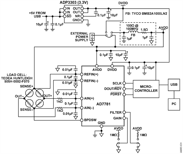
Since the AD7781 provides an integrated solution for weigh scales, it interfaces directly to the load cell. The only external components required are some filters on the analog inputs and capacitors on the reference pins for EMC purposes. The low level signal from the load cell is amplified by the AD7781’s internal PGA. The PGA is programmed to operate with a gain of 128. The conversions from the AD7781 are then sent to the PC using the USB interface where the digital information is converted to weight.
Figure 2 shows the actual test setup. A 6-wire load cell is used, as this gives the optimum system performance. A 6-wire load cell has two sense pins, in addition to the excitation, ground, and two output connections. The sense pins are connected to the high side and low side of the Wheatstone bridge. The voltage developed across the bridge can, therefore, be accurately measured regardless of the voltage drop due to the wiring resistance. In addition, the AD7781 has a differential analog input, and it accepts a differential reference. Connection of the load cell differential SENSE lines to the AD7781 reference inputs creates a ratiometric configuration that is immune to low frequency changes in the power supply excitation voltage.

With a 4-wire load cell, the sense pins are not present, and the ADC reference pins are connected to the excitation voltage and ground. With this arrangement, the system is not completely ratiometric because there will be a voltage drop between the excitation voltage and SENSE+ due to wiring resistance. There will also be a voltage drop due to wire resistance on the low side.
The AD7781 has separate analog and digital power supply pins. The analog and digital power supplies are independent of each other, so AVDD and DVDD can be at different potentials. The microcontroller uses a 3.3 V power supply. Therefore, DVDD is also powered from 3.3 V. This simplifies the interface between the ADC and the microcontroller because no external level shifting is required. The 3.3 V digital supply is generated using the ADP3303 (3.3 V) regulator.
There are several methods to power the weigh scale system. It can be powered from the main power supply bus or it can be powered from the ADP3303 (3.3 V). When the weigh scale is excited with 5 V, then the main power supply bus must be used. When exciting the load cell with 3.3 V, the main power supply bus or the ADP3303 (3.3 V) can be used. The ADP3303 (3.3 V) is a low noise regulator. In addition, noise reduction capacitors are placed on the regulator output as recommended in the ADP3303 (3.3 V) data sheet. To optimize the EMC, the regulator output is filtered before being supplied to the AD7781 and the load cell. It is essential that any regulators used to generate the power supply to the AD7781 and the load cell are low noise regulators, as any noise on the power supply or ground planes will introduce noise into the system and degrade the circuit performance.
If a 2 kg load cell with a sensitivity of 2 mV/V is used, the full-scale signal from the load cell is 10 mV when the excitation voltage is 5 V. A load cell has an offset, or TARE, associated with it. This TARE can have a magnitude that is up to 50% of the load cell full-scale output signal. The load cell also has a gain error that can be up to ±20% of full scale. Some customers use a DAC to remove or null the TARE. When the AD7781 uses a 5 V reference, its analog input range is equal to ±40 mV when the gain is set to 128. The wide analog input range of the AD7781 relative to the load cell full-scale signal (10 mV) is beneficial, as it ensures that the offset and gain error of the load cell do not overload the ADC’s front-end.
The AD7781 (C grade) has an rms noise of 49 nV when the output data rate is 10 Hz. The number of counts is equal to

where the factor of 6.6 converts the rms voltage into a peak-to-peak voltage. The resolution in grams is

The noise-free resolution is equal to

In practice, the load cell itself will introduce some noise. There will also be some time and temperature drift of the load cell along with the AD7781’s drift. To determine the accuracy of the complete system, the weigh scale can be connected to the PC via the USB connector. Using LabView software, the performance of the weigh scale system can be evaluated. Figure 3 shows measured output performance when a 1 kg weight is placed on the load cell and 500 conversions are gathered (5 V excitation voltage used). The noise of the system is calculated by the software to be 50 nV rms. This equates to 30,300 noise-free counts or 14.9 bits of noise-free code resolution.

Figure 4 shows the performance in terms of weight. The peak-to-peak variation in output is 0.075 grams over the 500 codes. So, the weigh scale system achieves an accuracy of 0.075 grams.

The plots show the actual (raw) conversions being read back from the AD7781 when the load cell is attached. In practice, a digital post filter is used in a weigh scale system. The additional averaging that is performed in the post filter will further im-prove the number of noise-free counts at the expense of a reduced data rate.
Common Variations
Note: The noise specifications given in this section are for a PGA gain of 128.
The AD7781 is a low noise, low power ADC for weigh scale design. Other suitable ADCs are the AD7798 and AD7780. The AD7780 has the same feature set as the AD7781, but it is a 24-bit ADC. The AD7798 allows a wider selection of output data rates. At 4.17 Hz, its rms noise is 40 nV.
For medium-end weigh scales, the AD7799 is a suitable device. At an output data rate of 4.17 Hz, the AD7799 has an rms noise of 27 nV.
For precision weigh scale design, the AD7190, AD7192, and AD7191 are suitable. The AD7190 has an rms noise of 8.5 nV when the output data rate is programmed to 4.7 Hz. It also offers a wide range of output data rates. It can operate up to 4.8 kHz and still maintain good performance. The AD7192 is pin-for-pin compatible with the AD7190. However, its rms noise is slightly higher. The AD7192 has an rms noise of 11 nV for an output data rate of 4.7 Hz. The AD7191 is a pin programmable device. It has four output data rates and four gain settings. Due to its pin programmability and reduced feature set, it is an easy to use device. Its rms noise is the same as the AD7192’s rms noise.
As with any high accuracy circuit, proper layout, grounding, and decoupling techniques must be employed. See Tutorial MT-031, Grounding Data Converters and Solving the Mystery of AGND and DGND and Tutorial MT-101, Decoupling Techniques for more details.
A complete design support documentation package for this circuit note can be found at the following address: http://www.analog.com/CN0108-DesignSupport.
Circuit Evaluation & Test
With the exception of the external load cell and the PC, the circuit of Figure 1 is contained on the AD7780 Evaluation Board (EVAL-AD7781EBZ ).
Interface to the evaluation board via a standard USB connector, J1. J1 is used to connect the evaluation board to the USB port of a PC. A standard USB connector cable is included with the AD7781 evaluation board to allow the evaluation board to interface with the USB port of the PC. Because the board is powered via the USB connector, there is no need for an external power supply, although if preferred, one may be connected via J2.
Equipment Needed
The EVAL-AD7781EBZ evaluation board and a PC running Windows 2000, Windows XP, or Windows Vista (32-bit) are the only items required other than the external load cell. A Tedea Huntleigh 505H-0002-F070 load cell was used to obtain the results presented in this circuit note. The load cell is not shipped with the evaluation board and must be purchased from the manufacturer by the customer.
Getting Started
The EVAL-AD7781EBZ evaluation board is shipped with a CD containing software that can be installed onto a standard PC to control the AD7781. The software communicates with the AD7781 through the USB cable, which accompanies the board. The software allows you to read conversion data from the AD7781. Data can be read from the AD7781 and displayed or stored for later analysis.
Install the AD7781 evaluation board software using the supplied AD7781 evaluation board CD before connecting the board to the PC. Complete details can be found in user guide UG-079.
Functional Block
Figure 1 of this circuit note shows the basic functional block diagram of the test setup.
Setup and Test
Complete instructions for setup and test of the AD7781 evaluation board can be found in user guide UG-079.
After installing the software, the AD7781 evaluation board should be configured for use with the external load cell by setting the appropriate links (jumpers) as described in Table 1 of UG-079. Make sure the links are set before applying power to the evaluation board.
The load cell connects to the evaluation board header J4. Operation of the Weighscale Demo is described in UG-079.


