AN-2558: RF Switch Performance with Arbitrary Loads
INTRODUCTION
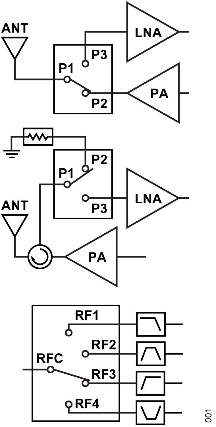
Radio frequency (RF) switches form a major building block in complex front-end systems for various applications including transmit or receive switching, diversity switching, band switching, and protection switching. Figure 1 shows the switch usage in typical RF signal chains. The location of the switch in the system architecture poses great demands on performance characteristics such as insertion loss, power handling, isolation, and switching speed. The RF switches by Analog Devices, Inc., which are implemented in the silicon on insulator (SOI) process, offer reflective, absorptive, and asymmetric functions that lead to higher frequency or power handling for wireless communications, aerospace or defense, and instrumentation applications.
RF switches usually consist of a series of on or off devices and shunt on or off devices that meet both insertion loss and isolation requirements as shown in Figure 2. On devices act like a resistor and off devices act like a capacitor, which determine the overall performance of the switch.

Although RF switches are designed and characterized for ideal 50 Ω conditions, real-world applications may or may not satisfy the preferred 50 Ω condition at all ports. Overall performance parameters, such as insertion loss and isolation, are dependent on the return loss magnitude and phase seen from the RF ports because the switch terminals are connected through a low resistance (<10 Ω). For example, a typical transmit/receive switch may be exposed to a 1:2 voltage standing wave ratio (VSWR) (~10 dB) from the antenna and ~10 dB return losses from a power amplifier or a low noise amplifier because the amplifiers are tuned for maximum power or minimum noise, which may be different from a high return loss 50 Ω termination.
This application note emphasizes the impacts of the arbitrary load conditions on insertion loss, isolation, and power handling using a load pull-based approach. End to end insertion loss and isolation degradation are possible because of poor return loss and arbitrary phase on RF ports. As for the power handling, arbitrary resistance and reactance on the RF port can cause voltage or current peaking, which may exceed the device limitations. Therefore, necessary derating for reliable operation is discussed.
PERFORMANCE UNDER POOR RETURN LOSS
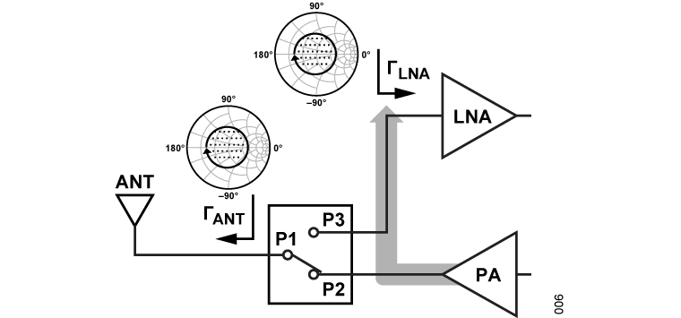
In a typical RF signal chain, the input and output ports of an RF switch rarely interface with ideal return loss components. RF components are commonly specified with a scalar return loss and an unknown phase as shown in Figure 3. Combined with an arbitrary RF trace length results in a random phase in a constant VSWR circle. As the return losses seen from the RF ports decrease, the uncertainty for insertion loss, isolation, and power handling increases.

MISMATCH LOSS
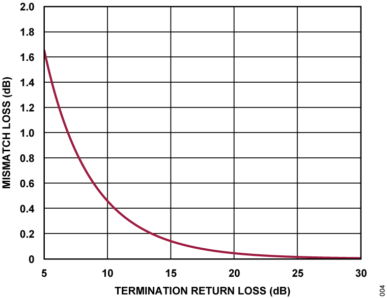
When ideal terminations are presented to the input and output of an RF switch, the inherent performance of a switch is observed optimally because there are no signal reflections. However, if a low return loss termination is presented, reflections occur and they add up to the inherent insertion loss of the switch, which is also known as mismatch loss. As shown in Figure 4, the mismatch loss increases as the termination return loss degrades. For example, a 10 dB return loss in the termination causes an additional ~0.45 dB mismatch loss to the system, whereas a 20 dB return loss corresponds to a ~0.05 dB mismatch loss.

To demonstrate the mismatch loss phenomena on a real device, the 20 W peak, 1 GHz to 20 GHz reflective switch ADRF5144 is experimented on. The ADRF5144 is an ideal transmit receive switch for high-power applications because of its high-power handling. On the other hand, the RF ports of the ADRF5144 are connected to an antenna, low noise amplifier (LNA), and power amplifier (PA), which can cause potential poor return loss.

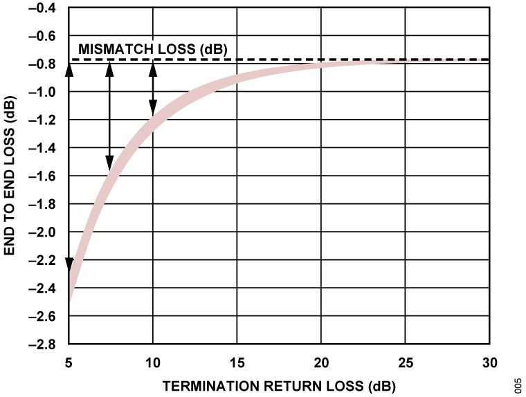
The ADRF5144 has a 0.8 dB insertion loss at 20 GHz when an ideal termination of 50 Ω is connected to its terminals. Figure 5 depicts the ADRF5144 insertion loss combined with the mismatch loss with respect to termination return loss. For an ideal case, such as a 30 dB termination return loss, a 0.8 dB insertion loss is obtained for any arbitrary phase. For a 20 dB return loss case, an additional 0.05 dB mismatch loss may be observed and for a 10 dB return loss case, an additional 0.45 dB mismatch loss is observed as expected from Figure 4.
ISOLATION UNDER POOR RETURN LOSS
Arbitrary load impedances not only affect the insertion loss, but also affect the leakage to the unselected arm of an RF switch, which is referred to as an isolation. The isolation performance of an RF switch is critical for certain applications such as transmit/receive switching, protection switching of delicate electronics such as a low noise amplifier (LNA), and filter bank switching. Terminations that have low return loss with an arbitrary phase can result in a higher leakage to the unselected RF arm.
A typical transmit/receive application scenario involves a 1:2 VSWR antenna, optimum noise matched LNA, and an optimum power matched PA where impedances are at 50 Ω. Likewise, in LNA protection applications, in addition to the antenna VSWR and LNA return loss, bulky 50 Ω termination resistors are commonly used to dissipate high power, which have poor return loss. As for the filter switching applications, out of band filter responses are usually full reflective, which require special attention. Depending on the application requirements, reflective or absorptive switches are a better fit to minimize the isolation uncertainties because of unknown load states.
Transmit/Receive Switch Application Example
Switches placed at the antenna interface are usually required to handle high power with as low insertion loss as possible for the selected path and as high isolation as possible for the unselected path for improved front-end performance. In a typical transmit scenario as shown in Figure 6, an increased uncertainty factor on the isolation can be observed because of low return loss and arbitrary phases seen from the switch ports. Therefore, worse isolation is observed.

For a typical PA to LNA leakage scenario, RFx to RFx isolation of a switch ideally depends only on the S32 parameter. However, when terminations are not ideal and return losses are low, reflections contribute to the total leakage of the transmit/receive switch as shown in Equation 1.

where:
PPA_to_LNA is the PA to LNA leakage.
ΓANT is the antenna reflection coefficient.
ΓLNA is the LNA reflection coefficient.
Figure 7 demonstrates the PA to LNA leakage for an ideal transmit/receive switch with respective to RFC to RFx (S31) and RFx to RFx (S32) isolation, when 10 dB return losses are present on the antenna and the LNA.

Figure 8 demonstrates how the isolation performance of a typical transmit/receive switch used at the front end varies with respect to arbitrary return loss and phase at its ports. The ADRF5144 has 49 dB RFx to RFx isolation and 43 dB RFC to RFx at 20 GHz, when measured with 50 Ω termination. The reflection back from a low return loss antenna contributes to the leakage uncertainty from transmit to receive minimally if LNA return loss is high. However, the leakage uncertainty increases when both antenna and LNA return losses are low with arbitrary phases. For example, the leakage uncertainty when both the antenna and the LNA have 20 dB return loss is 1.5 dB. However, when both the antenna and the LNA have 10 dB return loss and arbitrary phase, the uncertainty increases to 5 dB.

| Port Name | Return Loss Sweep | |
| Magnitude | Phase | |
| 20 dB LNA Input Return Loss (See Figure 8) | 20 dB | 0° to 360° |
| 10 dB LNA Input Return Loss (See Figure 8) | 10 dB | 0° to 360° |
| Antenna | 5 dB to 30 dB | 0° to 360° |
LNA Protection Example
Radio systems working on time division multiplexing (TDD) usually toggle LNAs and PAs complementary to each other where they share the same antenna via a circulator as shown in Figure 9. As a result, the receive path needs protection for certain high-power cases such as jamming, PA leakage, and antenna reflection. For these scenarios, protection switches are employed in front of the LNA, which must have minimal insertion loss and high-power handling capability. In protection mode, the switch is conducting to the external termination resistor, which is usually a bulky 50 Ω resistor. One expects high return loss from a 50 Ω termination but its return loss is not high at millimeter wave frequencies because of its large size and wide printed circuit board (PCB) pads. Therefore, leakage to the LNA is higher than expected.

For a typical circulator to LNA leakage scenario, RFC to RFx of a switch ideally depends only on the S31 parameter. However, when terminations and switch return losses are not high, reflections contribute to the total leakage of the switch as shown in Equation 2.

where:
PCIRC_to_LNA is the circulator to LNA leakage.
ΓTERM is the termination reflection coefficient.
ΓLNA is the LNA reflection coefficient.
Figure 10 demonstrates the circulator to LNA leakage for an ideal protection switch with respect to RFC to RFx (S31) and RFx to RFx (S32) isolation, when a realistic case of 15 dB return losses are present on the termination and LNA.

Figure 11 demonstrates the isolation performance at the ADRF5144 when there is a termination on the selected port. Because of the high-power handling requirements, termination resistors are not small in size and have bulky PCB pads. Unless further impedance matching is used, a typical high-power termination resistor at 20 GHz has 15 dB return loss. The arbitrary phase of the termination return loss and LNA return loss introduces an uncertainty on the common port to LNA leakage. A high 50 Ω at the termination may not be adequate to mitigate the uncertainty if the LNA return loss is low with the arbitrary phase. However, an inductive tuned termination resistor improves the isolation even though the LNA input return loss is low at arbitrary phase.

| Port Name | Return Loss Sweep | |
| Magnitude | Phase | |
| 15 dB/Arbitrary Phase Termination (See Figure 11) | 15 dB | 0° to 360° |
| 30 dB/Arbitrary Phase Termination (See Figure 11) | 30 dB | 0° to 360° |
| 15 dB/Inductive Phase Termination (See Figure 11) | 15 dB | 135° |
| LNA | 5 dB to 30 dB | 0° to 360° |
Filter Bank Switching Example
Filter switching applications are usually implemented with broadband back to back switches where narrow band bandpass filters are switched in and out as shown in Figure 12. Therefore, the leakage to the unselected channel is important. The overlooked scenario for the filter case is that the they are fully reflective out of band and return losses are very low, which needs special attention to assess the worst case signal leakage.

The ADRF5046 is a reflective SP4T and the ADRF5042 is an absorptive SP4T. As shown in Figure 13, a reflective switch has an isolation degradation uncertainty of ~10 dB with low return losses but an absorptive switch degrades only by ~3 dB. As power handling allows, absorptive switches provide higher inherent isolation, and their isolation performance are more tolerant to highly reactive low return losses.

POWER HANDLING UNDER POOR RETURN LOSS
Power rating of RF switches are usually limited by thermal or voltage breakdown of the devices along different paths inside the switch as shown in Figure 14. Thermal limitations are generally related to the on resistance of the RF field effect transistors (FETs), and voltage limitations are generally related to the breakdown of RF FETs, especially in off states. For terminated switches, an internal 50 Ω power handling is another limitation factor, which is thermal or voltage related depending on the architecture.

Thermal and voltage calculations are straightforward under ideal 50 Ω termination conditions. However, significant return losses on RF terminals with reactive components require further attention. When a low return loss termination is presented to the RF switch, the arbitrary impedance and phase can result peaking in voltage or current, which eventually leads to voltage induced breakdown or current induced thermal failures.

The ADRF5144 is rated up to 44 dBm peak power for terminations higher than 20 dB return loss, which is a typical limit with a standard lab setup and evaluation board configuration. For example, when the ADRF5144 is terminated with 20 dB return losses and driven with 44 dBm at 10 GHz, then a 57 V peak voltage or 1.1 A peak current may appear depending on the termination return loss phase. If a lower return loss load is presented to the switch, the voltage peaking or the current peaking is higher even though the source has the same RF power. The load pull chart in Figure 15 shows the constant voltage contours and constant current contours when different loads are presented to the switch. Given the arbitrary magnitude and phase of the load impedance, the voltage appearing on the switch varies from 30 V to 80 V, whereas the reliable peak voltage limit is below 57 V. Likewise, the current may scale between 0.6 A and 1.6 A, where the reliable peak current limit is below 1.1 A.

Figure 16 demonstrates the possible voltage peaking with respect to arbitrary termination return loss and phase if no derating is applied. As expected, the voltage peaking scales higher with respect to lower return losses although the input power is at a constant 44 dBm. To keep the voltage peaking at the allowed level, a derating is needed. Table 3 summarizes how the worst case possible voltage peaking levels scale for return loss and how much power rating is recommended for the ADRF5144. A more generalized derating approach is to follow Figure 17, where normalized derating values vs. termination return loss is shared as a guideline.
| Return Loss (dB) | Input Power (dBm) | Voltage (V) | Derating (dB) |
| 20 12 8 5 |
44 44 44 44 |
57 63 70 76 |
0 1 2 3 |
A more generalized approach that is used on any RF switch is to follow the recommended derating values shared in Figure 17.

SUMMARY
RF switch behavior under poor return loss requires further attention because the end to end insertion loss, isolation, and power handling specifications may vary with respect to return loss seen from RF ports. Application circuits of the latest high-power high-frequency switches by Analog Devices, such as the ADRF5144 or the ADRF5141, are optimized for different front-end scenarios to minimize the poor return loss impacts. Visit the Technical Support page for further recommendations.

