AN-1505: Using the AD7328 8-Channel ADC in Applications with Single-Ended Industrial-Level Signals
AN-1505: Using the AD7328 8-Channel ADC in Applications with Single-Ended Industrial-Level Signals
Circuit Function and Benefits
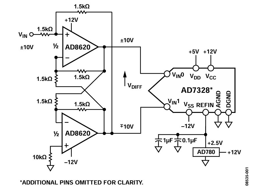
The circuit shown in Figure 1 is designed to optimize the performance of the AD7328 bipolar input, 8-channel, 12-bit plus sign analog-to-digital converter (ADC). The AD7328 can operate at a throughput rate of 1 MSPS. The selected operational amplifier (op amp) and reference voltage source ensure that maximum AD7328 performance is achieved with industrial level, single-ended signal sources by providing a low impedance driver with adequate settling time and an accurate reference supply.

The AD7328 is designed on the industrial complementary metal-oxide semiconductor (iCMOS®) process. This process combines high voltage silicon with submicron CMOS and complementary bipolar technologies. The AD7328 can accept true bipolar analog input signals. The AD7328 has four software selectable input ranges: ±10 V, ±5 V, ±2.5 V, and 0 V to +10 V. Each analog input channel can be independently programmed to one of the four input ranges. The analog input channels on the AD7328 can be programmed to be single-ended, true differential, or pseudo differential.
Circuit Description
In applications where harmonic distortion and signal-to-noise ratio are critical specifications, the analog input of the AD7328 must be driven from a low impedance source. Large source impedances significantly affect the ac performance of the ADC and can necessitate the use of an input buffer amplifier. When no amplifier is used to drive the analog input, it is recommended to limit the source impedance to low values. Due to the programmable nature of the analog inputs on the AD7328, the choice of op amp used to drive the inputs is a function of the particular application and depends on the input configuration and the analog input voltage ranges selected.
Differential operation requires that the VIN0 and VIN1 pins be driven simultaneously with two signals of equal amplitude that are 180° out of phase. Because not all applications have a signal preconditioned for differential operation, there is often a need to perform a single-ended to differential conversion. This single-ended to differential conversion can be performed using an op amp pair, as shown in Figure 1.
The AD8620 is an ideal choice of op amp that can be used to provide a single-ended to differential driver for the AD7328. The AD8620 is a precision, low input bias current, wide bandwidth junction field effect transistor (JFET) dual operational amplifier.
The circuit configuration shown in Figure 1 shows how an AD8620 op amp can be used to convert a single-ended signal to a differential signal that can be applied to the AD7328 analog inputs. The signals at points VIN+ and VIN− must have equal amplitude and be 180° out of phase.
The circuit accepts a bipolar ±10 V single-ended signal. The dual AD8620 amplifiers are connected in a cross coupled configuration to produce 20 V p-p signals at VIN1 and VIN that are 180° out of phase. Therefore, the differential input signal to the AD7328, VDIFF, is 40 V p-p. The cross coupled configuration provides for excellent phase match between the two outputs.
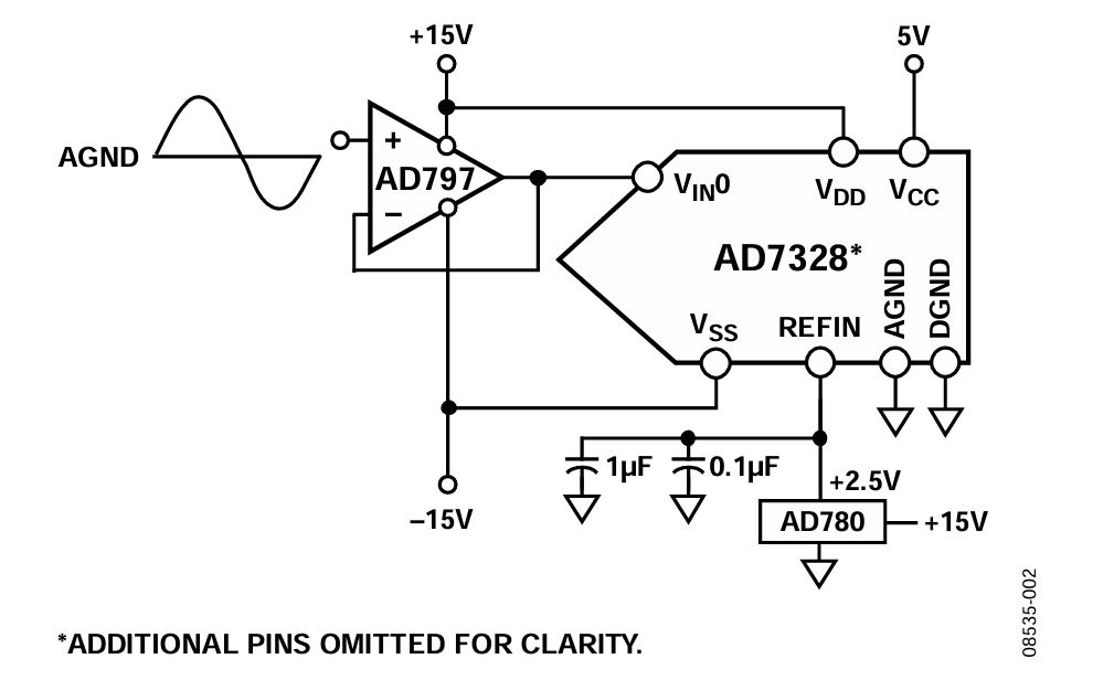
The AD7328 has a total of eight single-ended analog input channels. Figure 2 shows a typical connection diagram when operating the ADC in single-ended mode, where the AD797 is used to buffer the signal before applying it to the ADC analog inputs.

The analog input channels on the AD7328 can be independently programmed to accept one of four input ranges. The AD7328 can accept input signals of ±4 × VREFIN, ±2 × VREFIN, ±VREFIN, and 0 to +4 × VREFIN.
The AD7328 allows an external reference voltage to be applied to the REFIN/OUT pin. The specified voltage input range on the reference voltage is from 2.5 V to 3 V. Using 3 V reference voltages instead of 2.5 V allows the AD7328 to accept larger input signals. In Figure 1 and Figure 2, the AD780 is used as an external reference source. The AD780 is a 2.5 V/3 V ultrahigh precision voltage reference, which allows flexibility in the voltage range selected.
To achieve the specified performance, the circuit must be constructed on a multilayer printed circuit board (PCB) with a large area ground plane. Proper layout, grounding, and decoupling techniques must be used to achieve optimum performance (see the MT-031 Tutorial, the MT-101 Tutorial, and the EVALAD7328SDZ evaluation board layout).
Common Variations
Suitable voltage references for the AD7328 include the REF192, AD1582, ADR03, ADR381, ADR391, and ADR421. The AD8022 dual high speed, low noise op amp can also be used in high frequency applications where a dual op amp is desired. In high performance systems, a pair of AD8021 devices, a single-channel variant of the AD8022, can also be used in place of the AD8022. For lower frequency, single-ended applications, op amps such as the AD797 (single), the AD8610 (single), the AD8620 (dual), the AD8599 (dual), and the ADA4941-1 (differential), are suitable alternatives.
References
MT-036 Tutorial, Op Amp Output Phase-Reversal and Input Over-Voltage Protection. Analog Devices.
MT-074 Tutorial, Differential Drivers for Precision ADCs. Analog Devices.
MT-075 Tutorial, Differential Drivers for High Speed ADCs Overview. Analog Devices.