

ADP5054
RECOMMENDED FOR NEW DESIGNSQuad Buck Regulator Integrated Power Solution
- Part Models
- 1
- 1ku List Price
- Starting From $6.98
Overview
- Wide input voltage range: 4.5 V to 15.5 V
- ±1.5% output accuracy over full temperature range
- 250 kHz to 2 MHz adjustable switching frequency with individual ½× frequency option
- Power regulation
- Channel 1 and Channel 2
- Programmable 2 A/4 A/6 A sync buck regulators with low-side FET drivers
- Channel 3 and Channel 4: 2.5 A sync buck regulators
- Channel 1 and Channel 2
- Flexible parallel operation
- Single 12 A output (Channel 1 and Channel 2 in parallel)
- Single 5 A output (Channel 3 and Channel 4 in parallel)
- Low 1/f noise density
- 40 μV rms at 0.8 VREF for 10 Hz to 100 kHz
- Precision enable with 0.811 V accurate threshold
- Active output discharge switch
- FPWM/PSM mode selection
- Frequency synchronization input or output
- Power-good flag for Channel 1 output
- UVLO, OCP, and TSD protection
- 48-lead, 7 mm × 7 mm LFCSP
- −40°C to +125°C operational junctional temperature range
The ADP5054 combines four high performance buck regulators in a 48-lead LFCSP package that meets demanding performance and board space requirements. The device enables direct connection to high input voltages of up to 15.5 V with no preregulators.
Channel 1 and Channel 2 integrate high-side power metal-oxide semiconductor field effect transistors (MOSFETs) and low-side MOSFET drivers. External NFETs can be used in low-side power devices to achieve an efficiency optimized solution and to deliver a programmable output current of 2 A, 4 A, or 6 A. Combining Channel 1 and Channel 2 in a parallel configuration provides a single output with up to 12 A of current.
Channel 3 and Channel 4 integrate both high-side and low-side MOSFETs to deliver an output current of 2.5 A. Combining Channel 3 and Channel 4 in a parallel configuration can provide a single output with up to 5 A of current.
The switching frequency of the ADP5054 can be programmed or synchronized to an external clock from 250 kHz to 2 MHz, and an individual ½× frequency configuration is available for each channel.
The ADP5054 contains an individual precision enable pin on each channel for easy power-up sequencing. The internal low 1/f noise reference is implemented in the ADP5054 for noise sensitive applications.
Applications
- FPGA and processor applications
- Small cell base stations
- Security and surveillance
- Medical applications
Documentation
Data Sheet 1
User Guide 2
Brochure 1
Analog Dialogue 3
Webcast 2
ADI has always placed the highest emphasis on delivering products that meet the maximum levels of quality and reliability. We achieve this by incorporating quality and reliability checks in every scope of product and process design, and in the manufacturing process as well. "Zero defects" for shipped products is always our goal. View our quality and reliability program and certifications for more information.
| Part Model | Pin/Package Drawing | Documentation | CAD Symbols, Footprints, and 3D Models |
|---|---|---|---|
| ADP5054ACPZ-R7 | 48-Lead LFCSP (7mm x 7mm w/ EP) |
This is the most up-to-date revision of the Data Sheet.
Software Resources
Can't find the software or driver you need?
Request a Driver/SoftwareTools & Simulations
LTspice
Models for the following parts are available in LTspice:
- ADP5054
SIMPLIS Models 1
ADP505x Buck Regulator Design Tool
Microsoft Excel download tool from ADIsimPower to generate a power supply design complete with a schematic, bill of materials, and performance specifications.
Open ToolLTspice® is a powerful, fast and free simulation software, schematic capture and waveform viewer with enhancements and models for improving the simulation of analog circuits.
Evaluation Kits
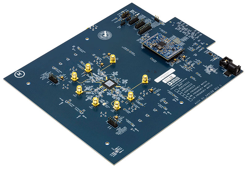
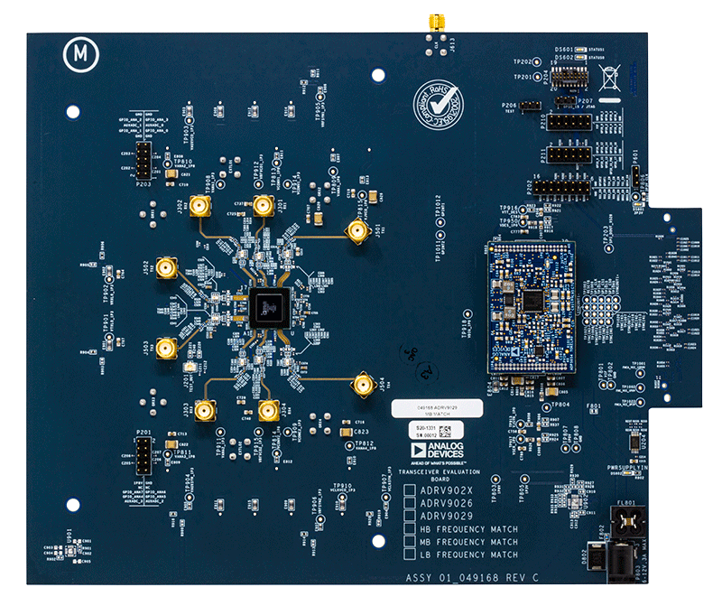
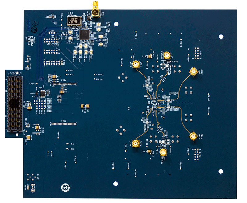
/ADRV9029
ADRV9022/ADRV906ADRV9029 Evaluation Board
Resources
/ADRV9029
ADRV9022/ADRV906ADRV9029 Evaluation Board
Resources
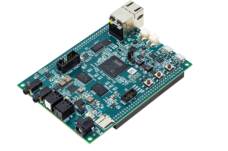
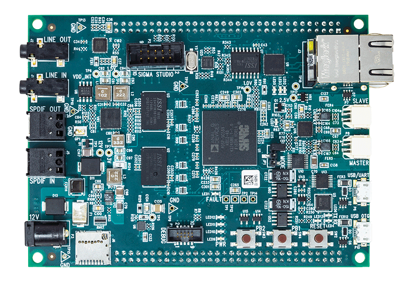
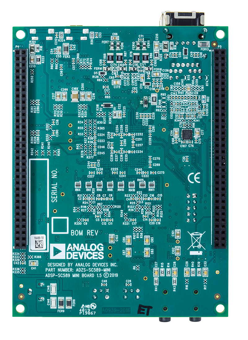
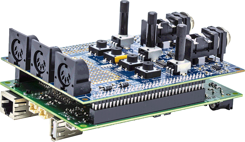
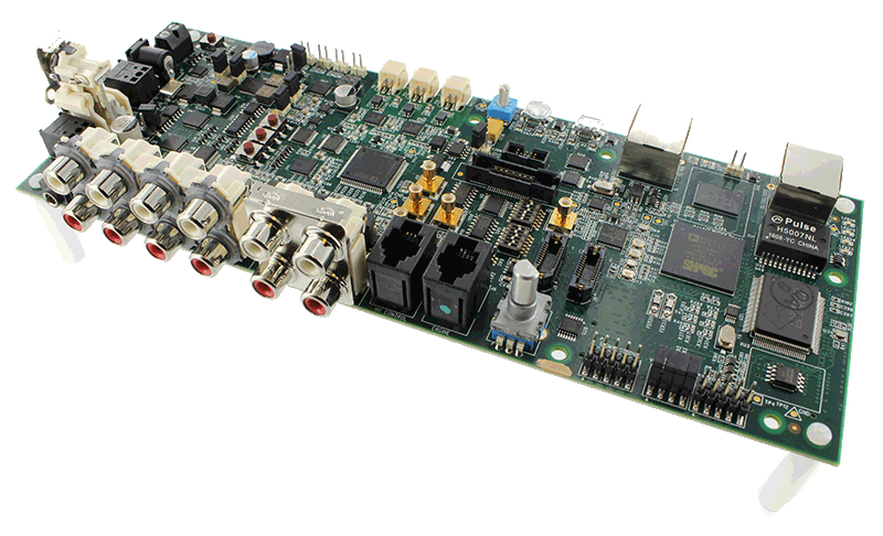
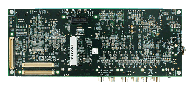
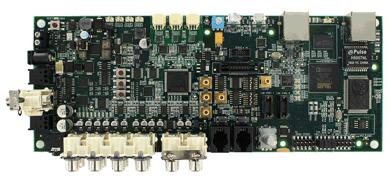
The SHARC Audio Module (SAM) is an expandable hardware/software platform for audio applications.
Resources
The SHARC Audio Module (SAM) is an expandable hardware/software platform for audio applications.
Resources
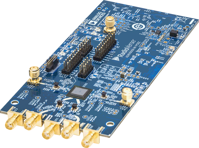
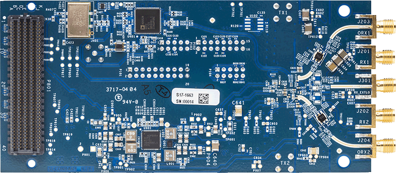
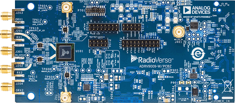
ADRV9008/ADRV9009 Evaluation Board
Resources
Software
ADRV9008/ADRV9009 Evaluation Board
Resources
Software
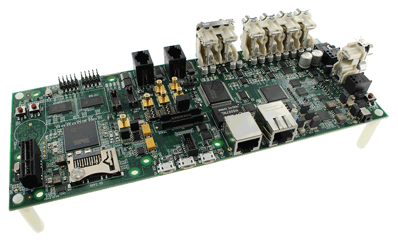
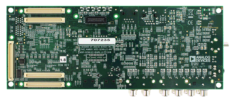
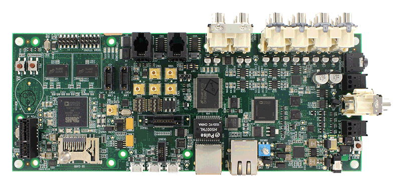
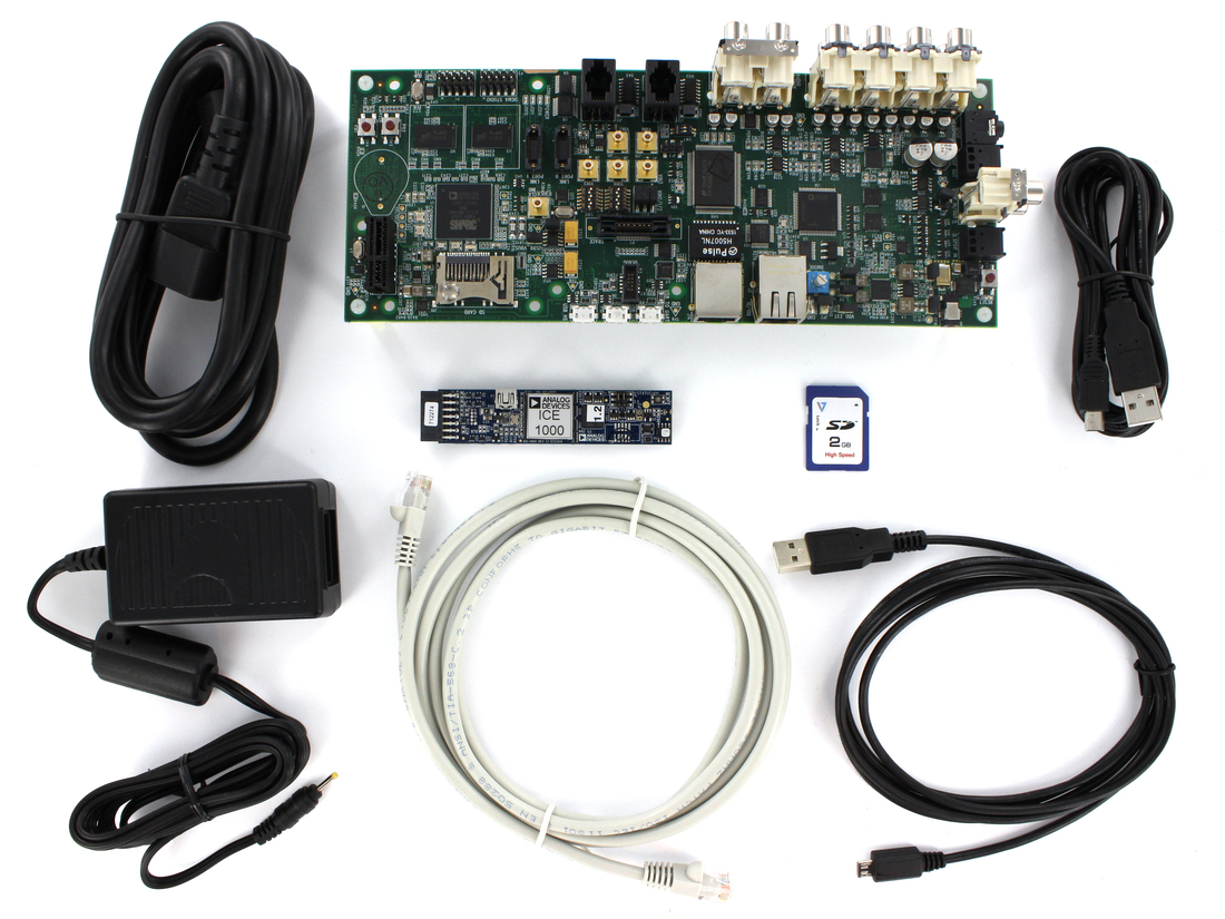
ADSP-SC589 Evaluation Hardware for the ADSP-SC58x/ADSP-2158x SHARC Family (529-ball CSPBGA)
Resources
ADSP-SC589 Evaluation Hardware for the ADSP-SC58x/ADSP-2158x SHARC Family (529-ball CSPBGA)
Resources
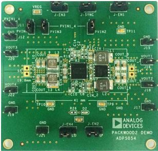
ADP5054 Evaluation Board
ADP5054 Evaluation Board
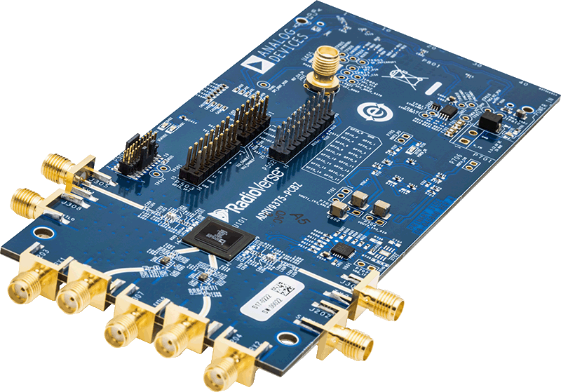
Evaluation Board
Resources
Software
Evaluation Board
Resources
Software
Evaluation Board
Features and Benefits
- Complete Radio Card platform containing AD9371 with:
- 2 x Transmit outputs
- 2 x Receive inputs
- 2 x Observation inputs
- 1x Sniffer path
- Narrow tuning range and Wide tuning range options
- ADRV9371-N/PCBZ matched for 1.8GHz – 2.6GHz
- ADRV9371-W/PCBZ matched for 300MHz – 6GHz
- Complete with high efficiency power supply solution and clocking solution for AD9371
- FMC connector to Xilinx ZC706 motherboard (EK-Z7-ZC706-G).
- Powered from single FMC connector
- Includes schematics, layout, BOM, HDL, drivers and application software
Product Details
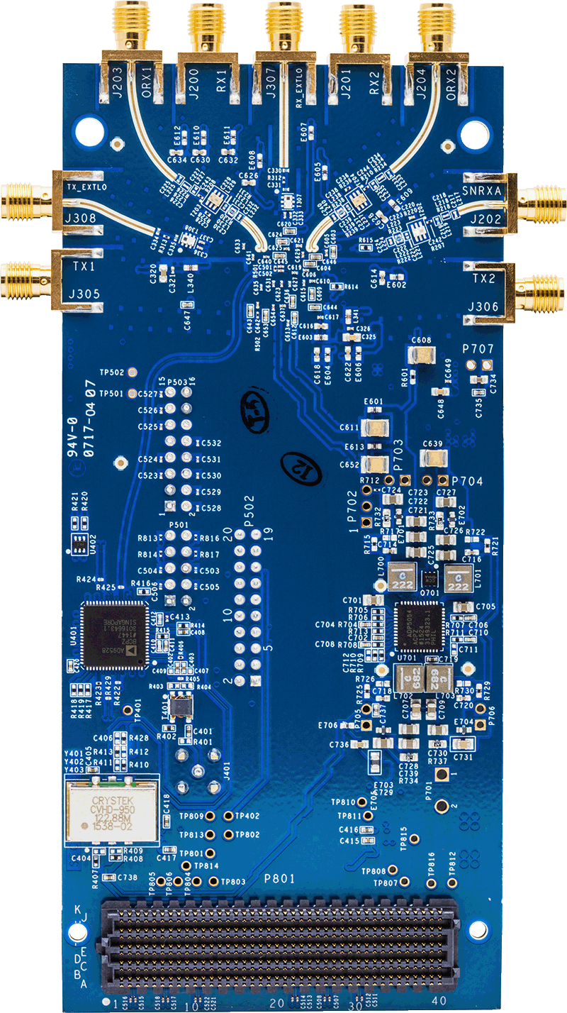
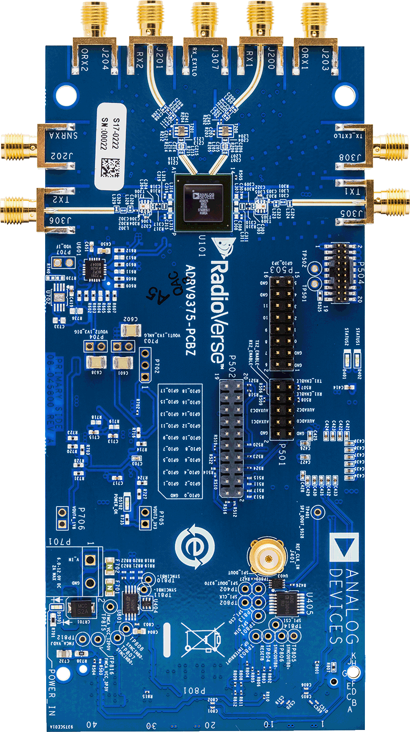
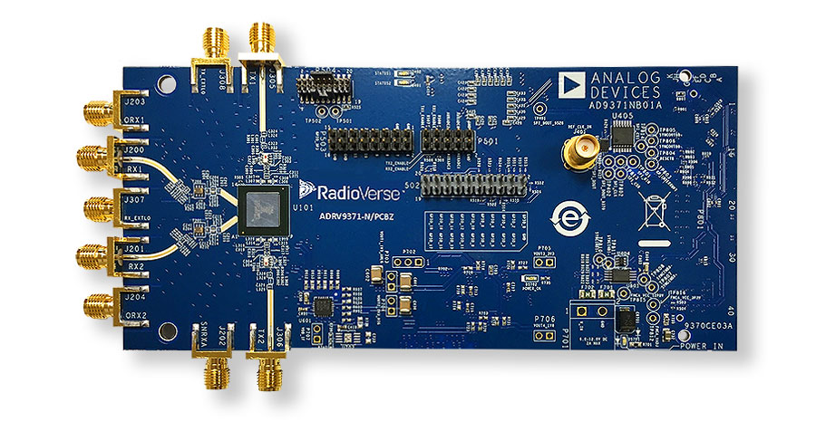
The ADRV9371-N/PCBZ and ADRV9371-WPCBZ are radio cards designed to showcase the AD9371, a high performance wideband integrated RF transceiver intended for use in RF applications such as 4G base station, test and measurement applications and software defined radios. The radio cards provide hardware engineers, software engineers and system architects with a single 2x2 transceiver platform for device evaluation and rapid prototyping of radio solutions. All peripherals necessary for the radio card to operate including a high efficiency switcher only power supply solution, and a high performance clocking solution are populated on the board.
Both narrow tuning range and wide tuning range options exist.
The ADRV9371-N/PCBZ is optimized for performance over a narrow tuning range1.8GHz – 2.6GHz. It will exhibit diminished RF performance on tuned RF frequencies outside of this band. This board is primarily intended to provide RF engineers with the ability to connect the AD9371 to an RF test bench (Vector Signal Analyzer, Signal Generator, etc.) and achieve its optimum performance.


The ADRV9371-W/PCBZ operates over a wide tuning range 300MHz – 6GHz, however the RF performance is tempered by the very wide band front end match. This board is primarily intended for system investigation and bringing up various waveforms from a software team before custom hardware is complete. The objective being for designers to see waveforms, but not being concerned about the last 1dB or 1% EVM of performance.


The board interfaces to the Xilinx ZC706 motherboard (EK-Z7-ZC706-G) (ordered separately).
Resources
Software
Evaluation Board
Features and Benefits
- Complete Radio Card platform containing AD9371 with:
- 2 x Transmit outputs
- 2 x Receive inputs
- 2 x Observation inputs
- 1x Sniffer path
- Narrow tuning range and Wide tuning range options
- ADRV9371-N/PCBZ matched for 1.8GHz – 2.6GHz
- ADRV9371-W/PCBZ matched for 300MHz – 6GHz
- Complete with high efficiency power supply solution and clocking solution for AD9371
- FMC connector to Xilinx ZC706 motherboard (EK-Z7-ZC706-G).
- Powered from single FMC connector
- Includes schematics, layout, BOM, HDL, drivers and application software
Product Details
The ADRV9371-N/PCBZ and ADRV9371-WPCBZ are radio cards designed to showcase the AD9371, a high performance wideband integrated RF transceiver intended for use in RF applications such as 4G base station, test and measurement applications and software defined radios. The radio cards provide hardware engineers, software engineers and system architects with a single 2x2 transceiver platform for device evaluation and rapid prototyping of radio solutions. All peripherals necessary for the radio card to operate including a high efficiency switcher only power supply solution, and a high performance clocking solution are populated on the board.
Both narrow tuning range and wide tuning range options exist.
The ADRV9371-N/PCBZ is optimized for performance over a narrow tuning range1.8GHz – 2.6GHz. It will exhibit diminished RF performance on tuned RF frequencies outside of this band. This board is primarily intended to provide RF engineers with the ability to connect the AD9371 to an RF test bench (Vector Signal Analyzer, Signal Generator, etc.) and achieve its optimum performance.
The ADRV9371-W/PCBZ operates over a wide tuning range 300MHz – 6GHz, however the RF performance is tempered by the very wide band front end match. This board is primarily intended for system investigation and bringing up various waveforms from a software team before custom hardware is complete. The objective being for designers to see waveforms, but not being concerned about the last 1dB or 1% EVM of performance.
The board interfaces to the Xilinx ZC706 motherboard (EK-Z7-ZC706-G) (ordered separately).
Resources
Software
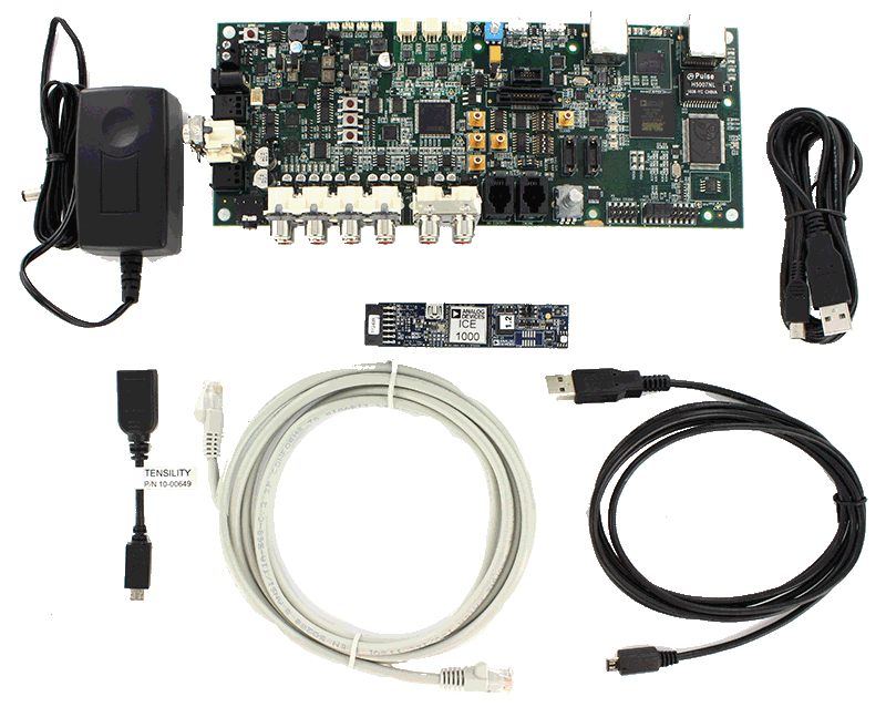
ADSP-SC584 Evaluation Hardware for the ADSP-SC58x/ADSP-2158x SHARC Family (349-ball CSPBGA)
Resources
ADSP-SC584 Evaluation Hardware for the ADSP-SC58x/ADSP-2158x SHARC Family (349-ball CSPBGA)
Resources
Reference Designs


Non-Hardware Verified Design