ADL8102

RECOMMENDED FOR NEW DESIGNS

GaAs, pHEMT, MMIC, Low Noise Amplifier, 1 GHz to 22 GHz

Viewing:

Overview

  • Single positive supply (self biased)
  • Gain: 27 dB typical at 9 GHz to 19 GHz
  • OP1dB: 13.5 dB typical at 1 GHz to 9 GHz
  • OIP3: 25 dBm typical at 1 GHz to 9 GHz
  • Noise figure: 2.5 dB typical at 9 GHz to 19 GHz
  • RoHS-compliant, 3 mm × 3 mm, 16-lead LFCSP
ADL8102
GaAs, pHEMT, MMIC, Low Noise Amplifier, 1 GHz to 22 GHz
ADL8102 - Functional Block Diagram ADL8102 - Pin Configuration
Add to myAnalog

Add product to the Products section of myAnalog (to receive notifications), to an existing project or to a new project.

Create New Project
Ask a Question

Documentation

Learn More
Add to myAnalog

Add media to the Resources section of myAnalog, to an existing project or to a new project.

Create New Project

Software Resources

EM-Plugs NEW

EM-Based RF Digital Twin Models

View Details

Tools & Simulations


Evaluation Kits

eval board
EVAL-ADL8102

Evaluating the ADL8102 Wideband, Low Noise Amplifier, Single Positive Supply, 1 GHz to 20 GHz

Features and Benefits

  • 2-layer Rogers 4350B evaluation board
  • End launch, 2.9 mm RF connectors
  • Through calibration path (depopulated)
  • Product Details

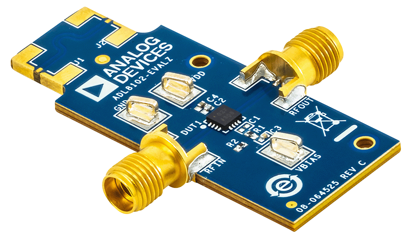
    The ADL8102-EVALZ is a 2-layer printed circuit board (PCB) fabricated from 10 mil thick, Rogers 4350B, and copper clad.

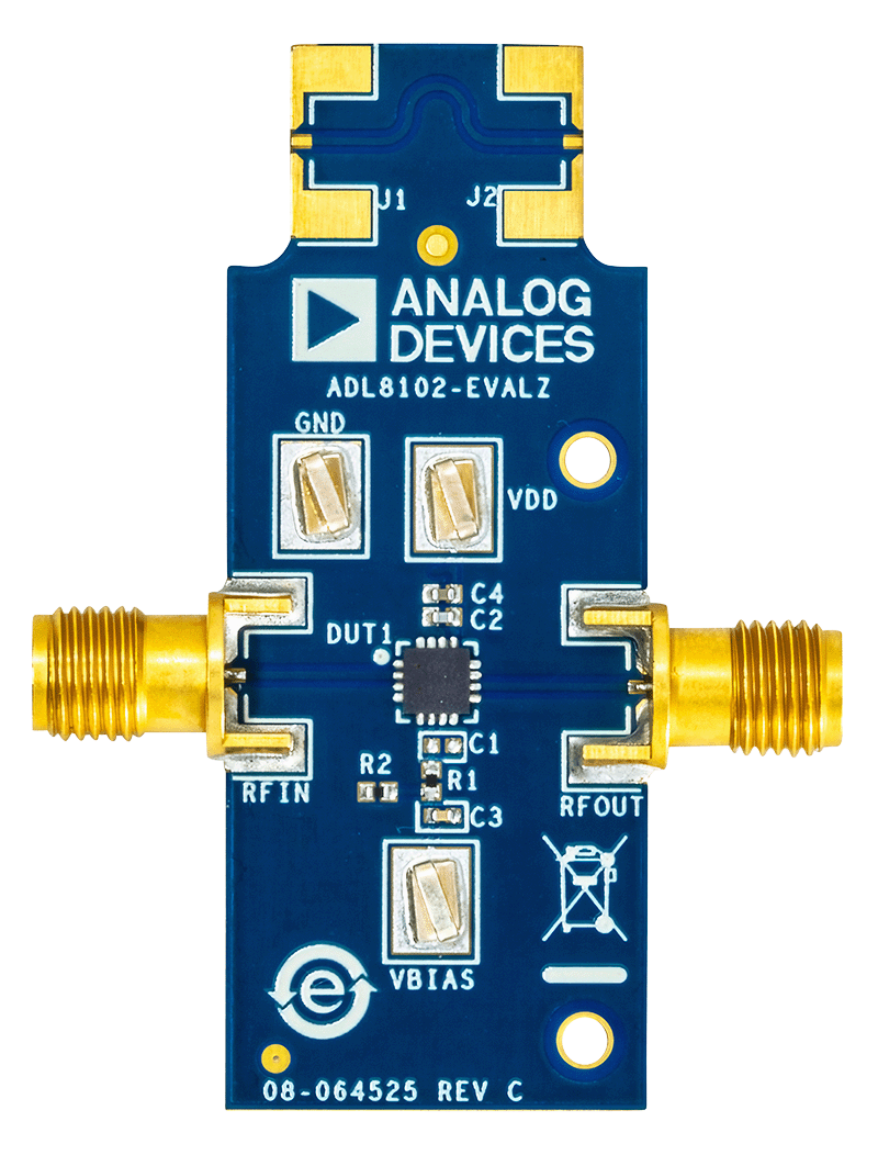
    The RFIN and RFOUT ports on the ADL8102-EVALZ are populated with 2.9 mm, female coaxial connectors, and the corresponding RF traces have a 50 Ω characteristic impedance. The ADL8102-EVALZ is populated with components suitable for use over the entire −40°C to +85°C operating temperature range.

    To calibrate board trace losses, a through calibration path, THRUCAL, is provided between the J1 and J2 connectors. J1 and J2 must be populated with RF connectors to use the through calibration path. For the through calibration path performance, see Table 1 and Figure 3 in the user guide.

    Access the ADL8102-EVALZ ground path and the VDD pin through the surface-mount technology (SMT) test point connectors, GND, and VDD. A supplementary test point for VBIAS is included for simple access on the RBIAS pin (for the test point locations, see Figure 5) in the user guide.

    The RF traces on the ADL8102-EVALZ are 50 Ω, grounded, coplanar waveguide. The package ground leads and the exposed pads connect directly to the ground plane. Multiple vias connect the top and bottom ground planes with particular focus on the area directly beneath the ground paddle to provide adequate electrical conduction and thermal conduction.

    The power-supply decoupling capacitors on the ADL8102-EVALZ represent the configuration used to characterize and qualify the device.

    Full specifications on the ADL8102 are available in the ADL8102 data sheet available from Analog Devices, Inc., and must be consulted with the user guide when using the ADL8102-EVALZ evaluation board.

    eval board
    ADXBAND16EBZ

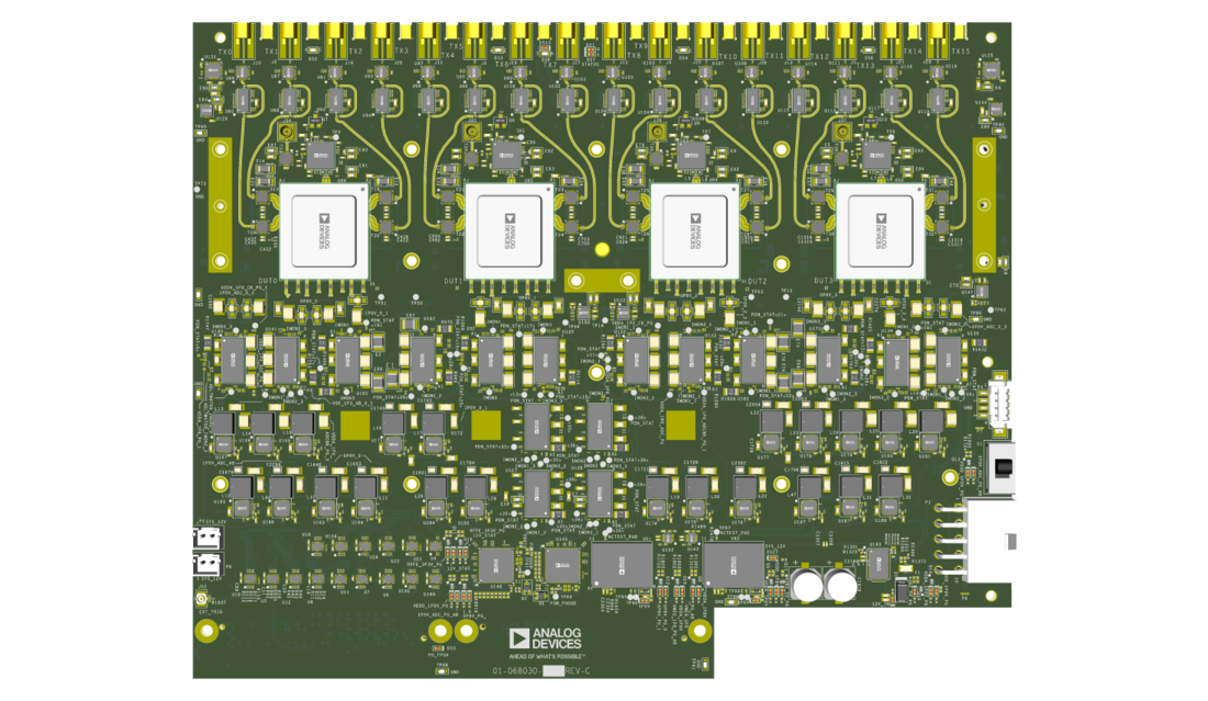
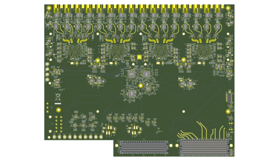
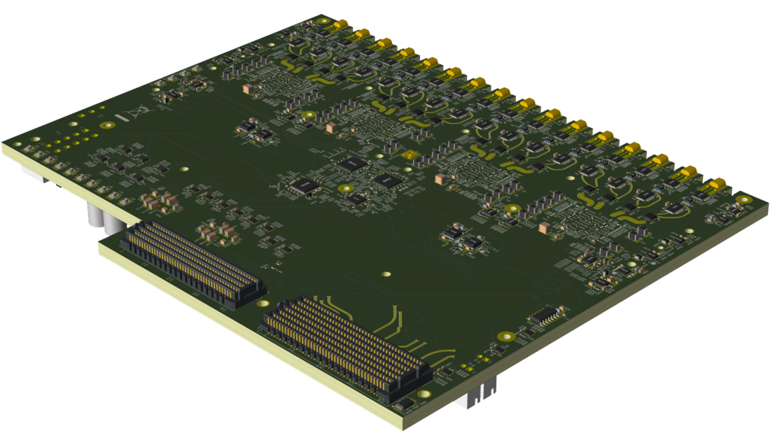
    16Tx/16Rx Direct X-Band Sampled Phased-Array/RADAR/SATCOM Development Platform

    Features and Benefits

    • Transmit and receive frequency X band: 8GHz to 12GHz
    • Direct sampling in L, S, and C bands with capacitor rotation
    • Multichannel, wideband system development platform for the AD9084 
    • Mates with Xilinx VCU118 evaluation board (must be purchased separately)
    • 16× RF receive channels (32× digital receive channels)
      • Total 16× 4GSPS to 20GSPS ADC channels
      • 48× digital downconverters (DDCs) and complex NCOs
      • 16× programmable finite impulse response filters (pFIRs)
      • 16× complex finite impulse response filters (CFIRs)
    • Complete power management solution for all domains
    • Single 12V supply voltage for easy power management
    • Board size: 221mm × 158mm (8.9” × 6.2”)

    Product Details

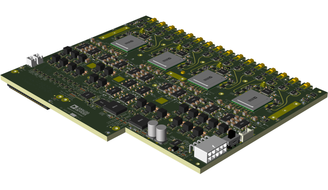
    This user guide serves as the main source of information for system engineers and software developers using the ADXBAND16EBZ. This platform contains four AD9084 software-defined, direct sampling mixed-signal front end (MxFE), including an RF front end, clocking, and power circuitry. Common target applications are phased array radars, electronic warfare, and ground-based SATCOM. The receive and transmit RF front ends have bypass configurations that allow customized frequency ranges of less than 8GHz up to 18GHz.

    The ADXBAND16EBZ highlights a complete system solution. This platform is intended as a testbed for demonstrating multichip synchronization as well as the implementation of system-level calibrations and signal processing algorithms. The system is designed to mate with a Xilinx VCU118 evaluation board, which features the Virtex UltraScale+ XCVU9P field-programmable gate array (FPGA), with provided reference software, hardware design language (HDL) code, and MATLAB system-level interfacing.

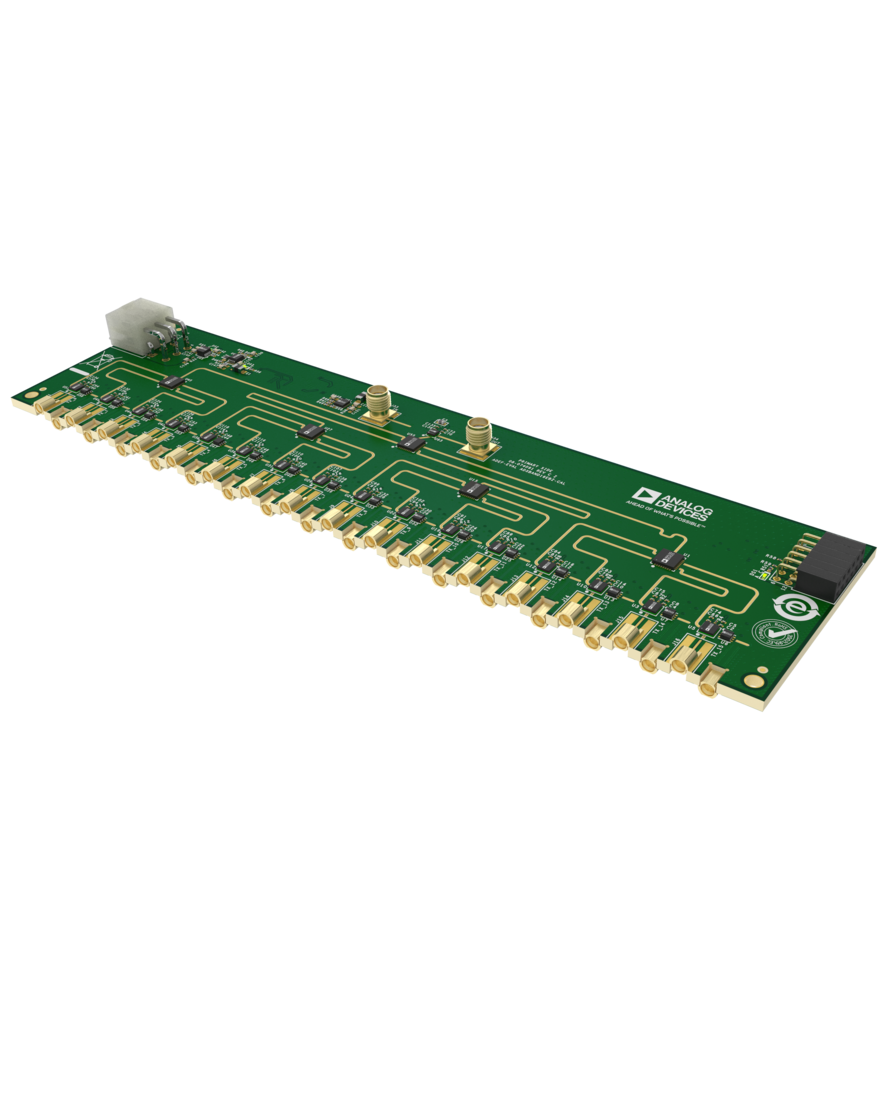
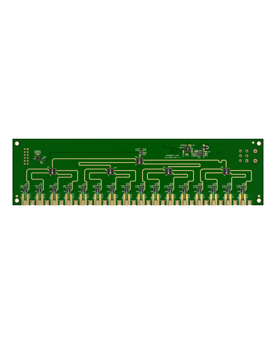
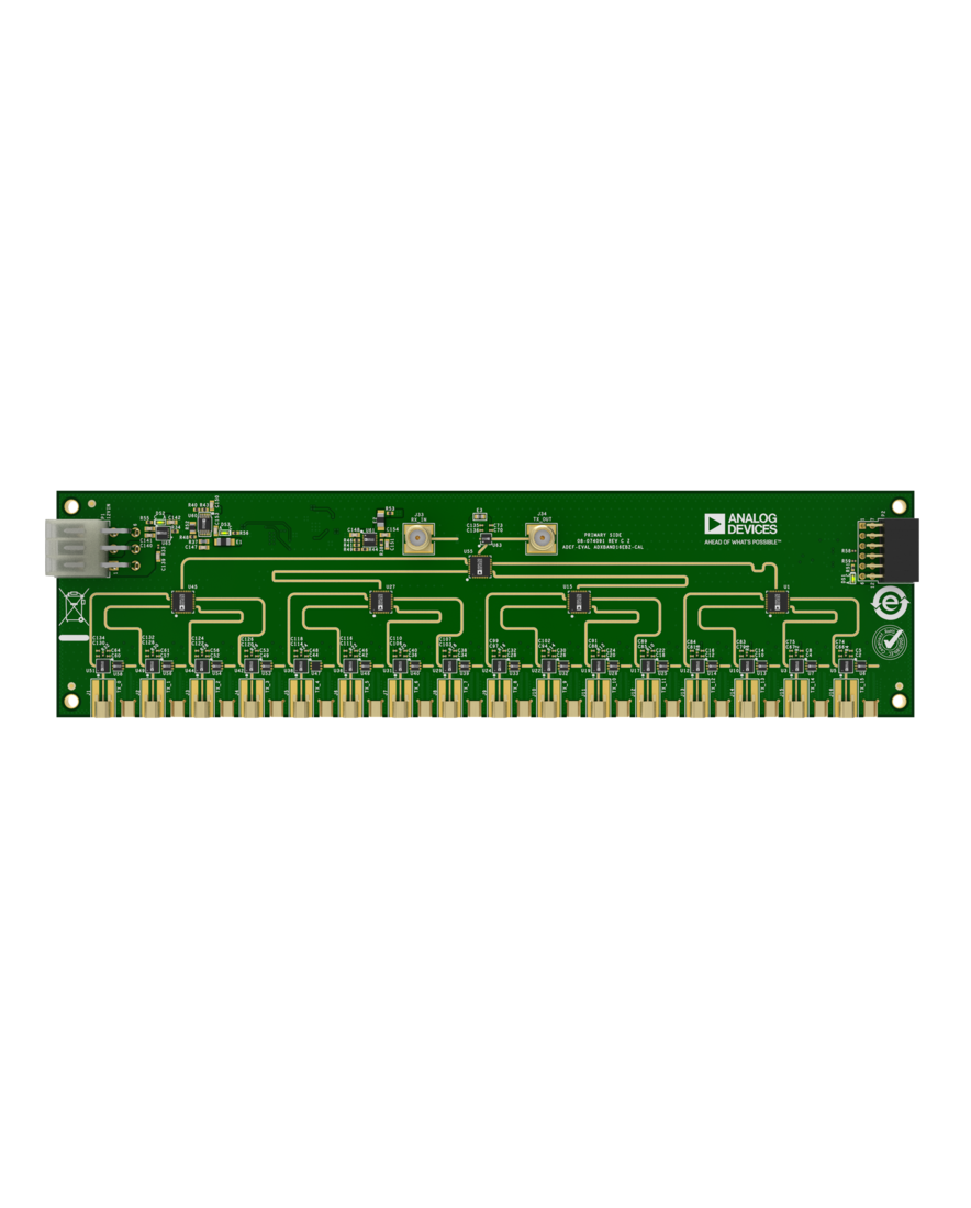
    A 16 transmit and 16 receive calibration board (ADXBAND16EBZCAL) can be used to develop system-level calibration algorithms to demonstrate power-up phase determinism. The calibration board demonstrates combined-channel dynamic range, spurious, and phase noise improvements that can also be controlled via a MATLAB add-on when connected to the peripheral module (PMOD) interface of the VCU118.

    APPLICATIONS

    • Phased-array, radar, electronic warfare, and satellite communications (SATCOM)
    • Communications infrastructure (multiband and mmWave 5G)
    • Electronic test and measurement

    EVAL-ADL8102
    Evaluating the ADL8102 Wideband, Low Noise Amplifier, Single Positive Supply, 1 GHz to 20 GHz
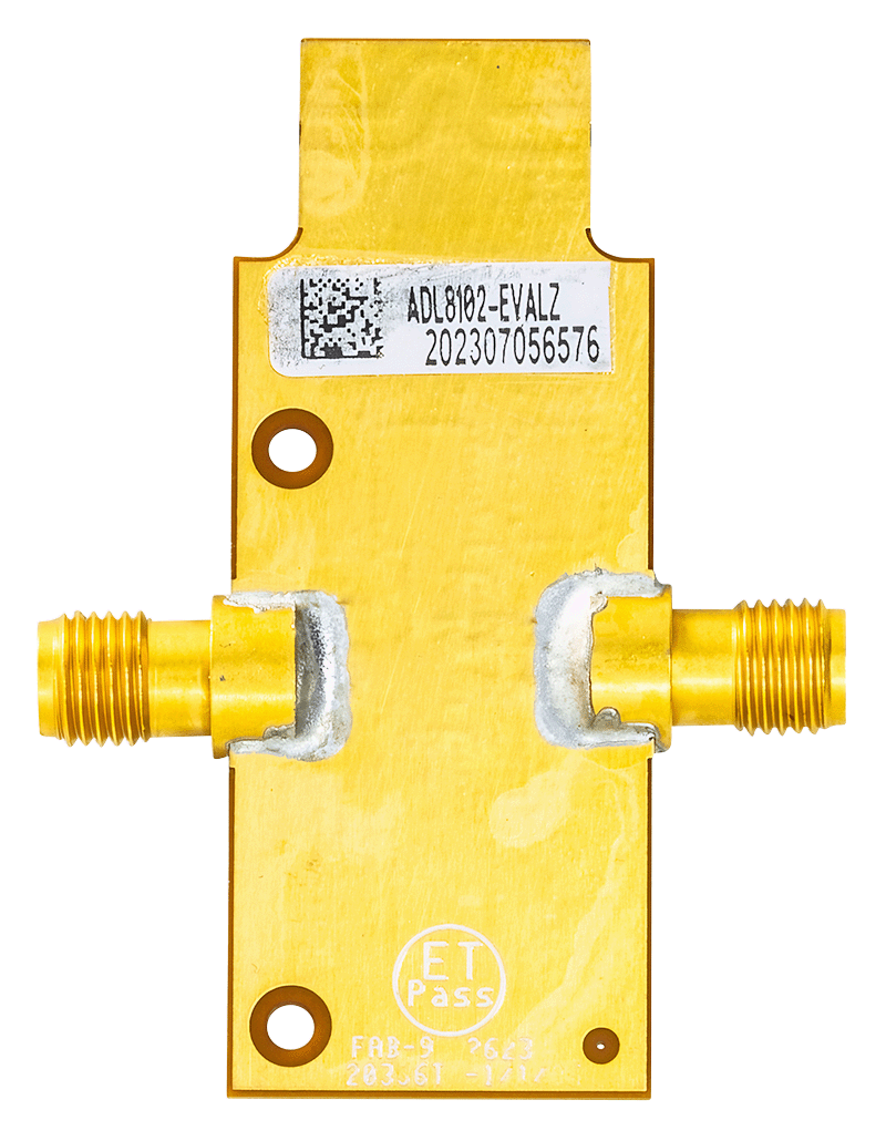
    ADL8102 Evaluation Board - Angle ADL8102 Evaluation Board - Top ADL8102 Evaluation Board - Bottom
    ADXBAND16EBZ
    16Tx/16Rx Direct X-Band Sampled Phased-Array/RADAR/SATCOM Development Platform
    ADXBAND16EBZ Top Angle Evaluation Board ADXBAND16EBZ Top Evaluation Board ADXBAND16EBZ Bottom Evaluation Board ADXBAND16EBZ Bottom Angle Evaluation Board

    Latest Discussions

    No discussions on ADL8102 yet. Have something to say?

    Start a Discussion on EngineerZone®

    Recently Viewed