

AD9217
RECOMMENDED FOR NEW DESIGNS12-Bit, 6 GSPS/10.25 GSPS, RF Analog-to-Digital Converter
- Part Models
- 2
- 1ku List Price
- Starting From $1629.61
Overview
- High instantaneous dynamic range
- NSD
- −155.1 dBFS/Hz at 10 GSPS with −9 dBFS, 170 MHz input
- −153 dBFS/Hz at 10 GSPS with −1 dBFS, 170 MHz input
- SFDR: 70 dBFS at 10 GSPS with −1 dBFS, 1000 MHz input
- SFDR excluding H2 and H3 (worst other spur): −89 dBFS at 10 GSPS with −1 dBFS, 1000 MHz input
- Low power dissipation: 4.2 W typical at 10 GSPS
- Integrated input buffer (6.5 GHz input bandwidth)
- 1.4 V p-p full-scale analog input with RIN = 50 Ω
- Overvoltage protection
- Low latency, high speed parallel output port
- Fast overrange detection for efficient AGC
- On-chip temperature sensor
- On-chip negative voltage generators
- Low CER: <1 × 10⁻¹⁶
- Reconfigurable support for AD9213 native mode
- 12 mm × 12 mm, 192-ball BGA-ED package
The AD9217 is a single, 12-bit, 6 GSPS/10.25 GSPS, radio frequency (RF) analog-to-digital converter (ADC) with a 6.5 GHz input bandwidth. The AD9217 supports high dynamic range frequency and time domain applications requiring wide instantaneous bandwidth and low conversion error rates (CER).
The AD9217 features a low latency, high speed, parallel CML output interface that supports full bandwidth operation with compatible FPGA/ASIC receivers. The AD9217 can be reconfigured to operate in native AD9213 mode for applications requiring additional digital processing and JESD204B output support. Refer to the AD9213 data sheet when operating the AD9217 in AD9213 mode.
The AD9217 achieves dynamic range and linearity performance while consuming 4.2 W typical. The device is based on an interleaved pipeline architecture and features a proprietary calibration and randomization technique that suppresses interleaving spurious artifacts into its noise floor. The linearity performance of the AD9217 is preserved by a combination of on-chip dithering and calibration, which results in excellent spurious-free performance over a wide range of input signal conditions.
The AD9217 is offered in a 192-ball ball grid array (BGA) package and is specified over a junction temperature range of −20°C to +115°C.
Documentation
Data Sheet 1
FPGA Interoperability Reports 1
Product Selection Guide 1
ADI has always placed the highest emphasis on delivering products that meet the maximum levels of quality and reliability. We achieve this by incorporating quality and reliability checks in every scope of product and process design, and in the manufacturing process as well. "Zero defects" for shipped products is always our goal. View our quality and reliability program and certifications for more information.
| Part Model | Pin/Package Drawing | Documentation | CAD Symbols, Footprints, and 3D Models |
|---|---|---|---|
| AD9217BBPZ-10G | 192-Ball BGA_ED (12mm x 12mm x 1.56mm w/ EP) | ||
| AD9217BBPZ-6G | 192-Ball BGA_ED (12mm x 12mm x 1.56mm w/ EP) |
This is the most up-to-date revision of the Data Sheet.
Software Resources
Can't find the software or driver you need?
Request a Driver/SoftwareEvaluation Kits

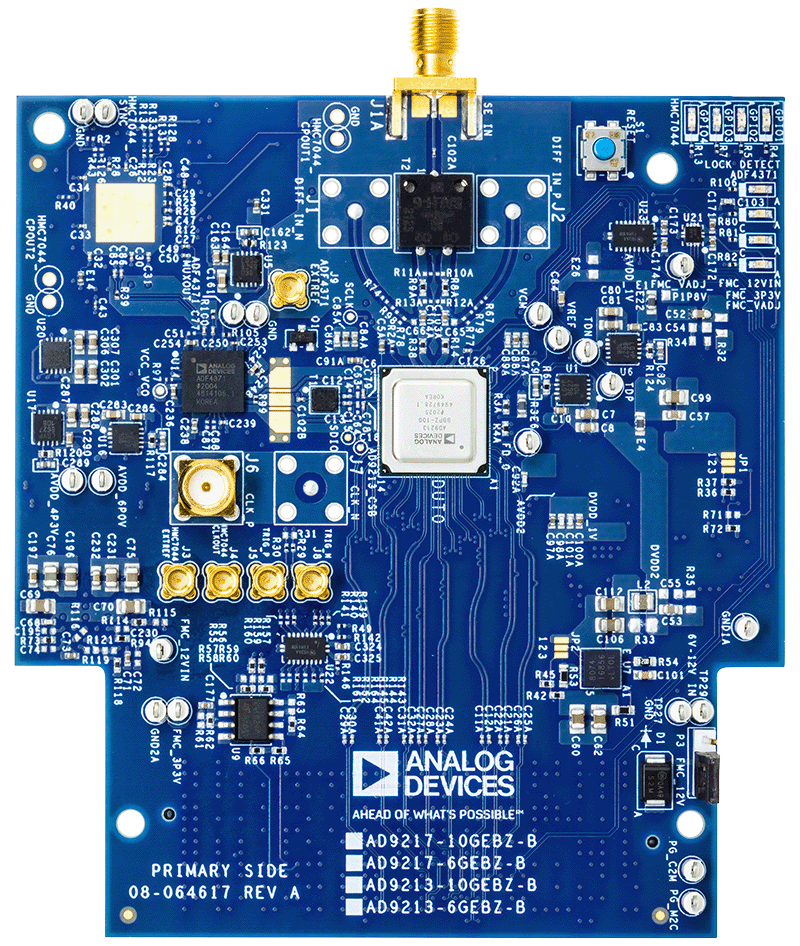

Quick Start Guide for Evaluating the AD9217 12-Bit, 6GSPS/10.25GSPS, RF ADC with the Customer Evaluation Board Using the ADS8-V1EBZ FPGA-Based Capture Board