AD7175-8
RECOMMENDED FOR NEW DESIGNS24-Bit, 8-/16-Channel, 250 kSPS, Sigma-Delta ADC with True Rail-to-Rail Buffers
- Part Models
- 3
- 1ku List Price
- Starting From $17.33
Overview
- Fast and flexible output rate: 5 SPS to 250 kSPS
- Performance specifications
17.2 noise free bits at 250 kSPS
20.2 noise free bits at 2.5 kSPS
24 noise free bits at 20 SPS
INL: ±1 ppm of FSR - 85 dB filter rejection of 50 Hz and 60 Hz with 50 ms settling
- 85 dB filter rejection of 50 Hz and 60 Hz with 50 ms settling
- User configurable input channels
8 fully differential channels or 16 single-ended channels
Crosspoint multiplexer
- Channel scan data rate of 50 kSPS/channel (20 µs settling)
- On-chip 2.5 V reference (±2 ppm/°C drift)
- True rail-to-rail analog and reference input buffers
- Internal or external clock
- Power supply: AVDD1 − AVSS = 5 V, AVDD2 = IOVDD = 2 V to 5 V (nominal)
Split supply with AVDD1/AVSS at ±2.5 V - ADC current: 8.4 mA
- Temperature range: −40°C to +105°C 3- or 4-wire serial digital interface (Schmitt trigger on SCLK) Serial port interface (SPI), QSPI, MICROWIRE, and DSP compatible
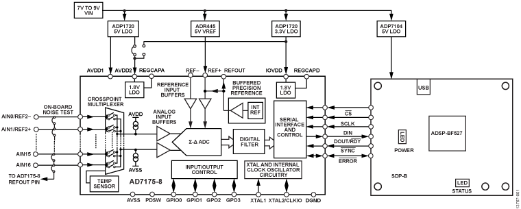
The AD7175-8 is a low noise, fast settling, multiplexed, 8-/16- channel (fully/pseudo differential) Σ-Δ analog-to-digital converter (ADC) for low bandwidth inputs. It has a maximum channel scan rate of 50 kSPS (20 µs) for fully settled data. The output data rates range from 5 SPS to 250 kSPS.
The AD7175-8 integrates key analog and digital signal condition-ing blocks to allow users to configure an individual setup for each analog input channel in use. Each feature can be user selected on a per channel basis. Integrated true rail-to-rail buffers on the analog inputs and external reference inputs provide easy to drive high impedance inputs. The precision 2.5 V low drift (2 ppm/°C) band gap internal reference (with output reference buffer) adds embedded functionality to reduce external component count.
The digital filter allows simultaneous 50 Hz and 60 Hz rejection at a 27.27 SPS output data rate. The user can switch between different filter options according to the demands of each channel in the application. The ADC automatically switches through each selected channel. Further digital processing functions include offset and gain calibration registers, configurable on a per channel basis.
The device operates with a 5 V AVDD1 . AVSS supply, or with ±2.5 V AVDD1/AVSS, and 2.5 V to 5 V AVDD2 and IOVDD supplies. The specified operating temperature range is .40°C to +105°C. The AD7175-8 is available in a 40-lead LFCSP package.
APPLICATIONS
- Process control: PLC/DCS modules
Temperature and pressure measurement - Medical and scientific multichannel instrumentation
- Chromatography
Documentation
Data Sheet 1
User Guide 2
Application Note 1
Technical Articles 1
Informational 1
Video 4
Circuit Note 2
Device Drivers 4
3rd Party Solutions 1
Analog Dialogue 1
Webcast 2
ADI has always placed the highest emphasis on delivering products that meet the maximum levels of quality and reliability. We achieve this by incorporating quality and reliability checks in every scope of product and process design, and in the manufacturing process as well. "Zero defects" for shipped products is always our goal. View our quality and reliability program and certifications for more information.
| Part Model | Pin/Package Drawing | Documentation | CAD Symbols, Footprints, and 3D Models |
|---|---|---|---|
| AD7175-8BCPZ | 40-Lead LFCSP (6mm x 6mm w/ EP) | ||
| AD7175-8BCPZ-RL | 40-Lead LFCSP (6mm x 6mm w/ EP) | ||
| AD7175-8BCPZ-RL7 | 40-Lead LFCSP (6mm x 6mm w/ EP) |
| Part Models | Product Lifecycle | PCN |
|---|---|---|
|
Jul 22, 2025 - 25_0055 Gold Wire to Copper Wire Conversion(PCA) |
||
| AD7175-8BCPZ | PRODUCTION | |
| AD7175-8BCPZ-RL | PRODUCTION | |
| AD7175-8BCPZ-RL7 | PRODUCTION | |
This is the most up-to-date revision of the Data Sheet.
Software Resources
Mbed Support 5
Device Drivers 4
Evaluation Software 1
AD717x Eval+ Software
Can't find the software or driver you need?
Tools & Simulations
Virtual Eval - BETA
Virtual Eval is a web application to assist designers in product evaluation of ADCs, DACs, and other ADI products. Using detailed models on Analog’s servers, Virtual Eval simulates crucial part performance characteristics within seconds. Configure operating conditions such as input tones and external jitter, as well as device features like gain or digital down-conversion. Performance characteristics include noise, distortion, and resolution, FFTs, timing diagrams, response plots, and more.
Open ToolIBIS Model 1
ADI Circuit Explorer™
ADI Circuit Explorer™ uses AI to interpret natural language prompts and search a database of validated analog circuit designs, helping you quickly find the best match for your needs.
Open ToolSignal Chain Designer
Signal Chain Designer is a web-based tool designed to create and simulate complex precision signal chains. See your circuit’s performance before you commit to your PCB: transfer function, noise, power consumption, input range, and DC error. Quickly experiment with different parts and architectures. Signal chains can be exported to LTspice for further analysis.
Open ToolEvaluation Kits
Latest Discussions
No discussions on AD7175-8 yet. Have something to say?
Start a Discussion on EngineerZone®


