One of the key benefits of modern SAR and Σ-Δ analog-to-digital converters (ADCs) is that they are designed with ease of use in mind, where ease of use was an afterthought for previous generations. This simplifies the task for system designers and, in many instances, allows for a single reference design to be used and recycled for multiple generations and across a great variety of applications. In many instances, it allows you to build one reference design that can be used for different applications over a long period of time. The hardware of a precision measurement system stays the same while the software implementation adapts to the different system needs. That’s the beauty of reusability, but nothing in life is entirely advantageous—there’s always a penalty. The primary drawback to having a single design for multiple applications is that you forego the customizations and optimizations necessary to achieve the absolute highest possible performance for dc, seismic, audio, and higher bandwidth applications. In the rush to reuse and complete designs, precision performance is often sacrificed. One of the primary oversights and areas of neglect is in clocking. In this article, we will discuss the importance of the clock and offer guidance on proper designs for high performance converters.
ADC Fundamentals
Relation Between Jitter and Signal to Noise Ratio
When looking at the available literature, the dependency of ADC performance on the jitter specification is well described and, usually for good reason, such titles includes the words “high speed.”1 To examine the relationship between jitter and signal-to-noise ratio (SNR), the starting point is the relationship between the SNR figure and the rms jitter.
If jitter is the primary source of noise in the system, this relationship simplifies to:

If there are different sources of noise contributing, you need to use Equation 2 to calculate the combined SNR:

Where:
A, Fin—parameters of input signal, amplitude, and input frequency
ev is simplified voltage noise rms
δtRMS is total rms jitter estimated as the rms sum of various contributions:

For in depth tutorial of Equation 3 usage see: analog.com/MT-008.
The summing is valid on uncorrelated noise sources. With Equation 2, we show the SNR depending on thermal noise (e²v) and jitter noise. The jitter contribution to SNR is dependent on the input frequency (fIN). This means at higher frequencies, the SNR is mainly defined by the jitter. Figure 1 includes the curves from Equation 1 and Equation 2 for ideal and real-life ADCs affected by jitter. Plots such as Figure 1 are common for high speed ADC data sheets, but they generally start in the MHz range. For precision ADCs, we will show the same dependencies further down in the kHz ranges. We are pushing SNRs in excess of 108 dB (see Figure 1), which precision ADCs are capable of nowadays. This is where the AD7768-1 comes in handy.

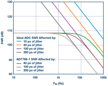
Upon review of the plot in Figure 1, you can see that the AD7768-1 converting a 1 kHz signal (gray line) will be affected by clock jitter only if σtRMS exceeds 300 ps. We can rearrange variables and show jitter requirement for specific ENOB and fIN:


Target jitter for nowadays high precision converters will prevent the designer from using common relaxation oscillators (like the 555 timer-based oscillator) or many microcontroller or FPGA-based clock generators. This leaves us with crystal (XTAL) and phase-locked loop (PLL) oscillators. New technological advances in MEMS oscillators will be suitable as well.
Can Oversample Techniques Help Here?
An important observation in Equation 1 and Equation 2 is that there is no explicit dependency on the sampling frequency. This tells us that the contribution of jitter will be hard to mitigate with oversampling techniques (plain or noise shaped). Oversampling is very common in high precision systems, but offers almost nothing to fight in terms of jitter noise. Relation to the sampling frequency can be found in Equation 4:

Where:
L(f) is the phase noise spectral single-sideband (SSB) density function
fmin and fmax are the frequency span relevant to the particular measurement.
For in depth tutorial of Equation 4 usage see: analog.com/MT-008.
Generally, jitter contribution should be considered only poorly improved by increasing fS.2 In theoretical discussions, the oversampling ratio of an ADC offers some reduction of broadband jitter contributions.3 For quantization and thermal noise, noise shaping is a very efficient way of suppressing noise in the band of interest. Increasing oversampling ratios suppresses quantization noise a lot faster (Equation 5) than noise jitter suppression as shown in Equation 6. This makes jitter stand out even more in oversampling structures that utilize noise shaping. In Nyquist converters, this might not pronounce itself as severely. Figure 3 illustrates this phenomenon using the example of a second-order Σ-Δ ADC and a new, forth-order Σ-Δ ADC.
The relation between quantization noise shaped by an Nth-order shaper with base error Δ at oversampling ratio M:

The relation between the oversampling ratio M and the amount of jitter:

Equation 7 shows the second-order noise shaping (N = 2). Your attention should go to M as it changes now with the power of 5.


Universal relations will be seen on different generations of converters. A first-order noise shaper will hide jitter for the longest time, progressing with a cubic relation to ~1/M3, whereas a fourth-order Σ-Δ will get us to the relation of ~1/M9. Jitter, at best, will be reduced by 1/M, and this generously assumes the presence of strong wideband frequency components as opposed to the relation of 1/(fN).
Will the Amplitude of the Signal Change Things?
Equation 2 shows that amplitude is in both the numerator and the denominator, preventing good trade off between the amplitudes and the SNR figure. One can make the SNR worse with attenuated signal where, in addition to jitter, thermal noise starts to limit the dynamic range. So, we can see new precision ADCs will be exposed to jitter restrictions in almost all but dc/seismic applications if pushed to achieve low enough noise.
Clock Jitter Will Have a Spectrum Too
In the introduction, we established the relationship between the signal, the overall voltage noise, and the rms of clock jitter. The SNR figure connects those three in a fairly straightforward Equation 2. The SNR figure is a good benchmark to compare circuits, but it doesn’t necessarily determine usability in actual applications. In many applications, designing especially for SNR isn’t good enough. For those interested in those specifications, spurious free dynamic range (SFDR) becomes the design target. In new high precision systems, 140 dB or even 150 dB of SFDR is achievable.
The process where a signal is distorted by a clock source can be examined by looking at it as mixing both. For analysis in frequency domain, FM modulation theory is employed.3 The resulting fast Fourier transform (FFT) spectrum is a product of mixing clock source spectrum with the input signal spectrum. To review how our ADC is affected by this, we introduce phase noise. Jitter and phase noise describe the same phenomena, but, depending on the application, one will be preferred. We have already shown how translation between phase noises into jitter figures can be done in Equation 3. In the integration process, spectral nuances will be lost.


Phase noise density plots are commonly supplied with clock source equipment and PLL specifications. Plots such as Figure 4 become more scarce for lower frequency sources, which are used in current oversampling converters and total jitter (rms or peak) is reported instead.
Resistor and transistor elements can be forced to exhibit fairly flat noise behavior near dc with chopping schemes. There is no equivalent of chopping for clock circuits available.
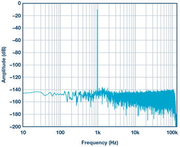
When converting a high amplitude AIN signal, the resulting FFT becomes an FM modulated spectrum, where AIN acts as the carrier and the clock sidebands are equivalent to the signal. Note that phase noise will not be band-limited in your FFT and noise will simply deposit multiple alias contributions in slices (see Figure 6).
In precision ADCs, one can usually rely on the natural decaying nature of phase noise and not provide any clock antialiasing filter. There is some scope for jitter reduction by adding filtering to the clock source—for example, using a tuned transformer in the clock path to exhibit a desirable frequency response. Finding out upper integration bound for integral frequency (Equation 4) is not easy to pinpoint. Precision ADC data sheets do not provide much advice on this. In those circumstances, engineering assumptions are made about clock CMOS inputs.
A more common problem in precision ADCs happens very near the fIN frequency where a 1/(fN) shape of phase noise will deteriorate SFDR. A large AIN signal will act as a blocker—a term more popular in radio receivers which is also applicable here.
When aiming to record high precision spectrums with very long capture times, SFDR will suffer greatly due to the nature of clock phase noise spectral density. The SNR and a visual FFT plot can be improved by shorter capture times (wider frequency bins). For a given FFT capture, rms jitter should be counted as integrated phase noise from ½ of the bin frequency. This becomes obvious upon review of Figure 5.


While this trick may visually improve FFT plots and SNR figures, it will do nothing for the observation of signals near the blocker. An important generalization and simplification of FM modulation equations is that heights of skirts are proportional to the ratio in Equation 8:

Elongating integration time for a single FFT hit is an uphill battle to collect further and more pronounced sections of phase noise. One will need to consider alternative ways of combining longer captures to improve this.


For practical purposes, SSB plots should be compared at a single point at fBIN/2 offset frequency to pick a better source for clean, close-in spectrum and SFDR. If comparing sources to achieve better SNR, then integration in Equation 4 needs to be performed from fBIN/2 to more than 3× fS (jitter aliases).
Sigma-Delta Modulators’ Sensitivities to Clocks
The previous topics are universal for any ADC regardless of architecture and technology. The following topic will deal with challenges presented by specific technologies. One of the most prominent examples of jitter dependency is inside Σ-Δ ADCs. The distinction between discreet time and continuous time operation of modulators will have tremendous influence on jitter immunity.
Continuous and discrete time Σ-Δ ADCs suffer not only due to sampling-related jitter contribution, but also the fact that their feedback loops can be significantly disrupted by jitter. Linearity of DAC elements in both discrete time and continuous time modulators is key to achieving high performance. Intuitive understanding of the DAC’s significance can be illustrated by drawing parallel to an operational amplifier (op amp). If one is tasked with designing a voltage amplifier with gain equal to 2, the first draft of anyone with a fundamental understanding of circuit design will be an op amp and two resistors. If external circumstances are not extreme, the circuit shown in Figure 7a will do its job. For the most part, the circuit designer doesn’t have to understand op amps in order to achieve great performance. The designer has to pick resistors that are well matched and precise enough to achieve the right gain. For noise purposes, they have to be small. For thermal behavior, the thermal coefficients need to match. Note that none of these dependencies are dictated by the op amp. Op amp nonidealities are secondary for this circuit operation. Yes, the influence of input current or capacitive load can be devastating. The ability to slew needs to be reviewed as there might be noise contributions to consider if the bandwidth is not limited. But you only get to fix those problems if you haven’t stunted your performance by choosing the wrong resistors. In Σ-Δ ADCs, feedback is more complicated than two resistors—in those circuits, we have DACs instead of resistors performing the corresponding function. Flaws in DAC operation are very detrimental while the remainder of the circuit will reap the benefits of loop-gain in a manner similar to op amp circuits.


ADCs employ element shuffling, or calibrations, which provides a way to deal with mismatches of DAC elements. Those will move errors into high frequency, but will also use a lot more timed events with the potential to increase jitter-related deterioration. This leads to a situation where the noise floor will be polluted by jitter contribution, reducing the effectiveness of noise shaping. Since modulators can employ different DAC schemes—and their mixes—such as return to zero and half return to zero. It is beyond the scope of this article to drill down into analysis and numerical simulations of those schemes.
With regards to jitter in this article, we will limit ourselves to pictorial simplifications. Since jitter dependency problems are within ADC loops, some new designs will provide frequency multipliers on silicon that are designed with an appropriate amount of phase noise. While this takes away a chunk of the work from system designers, please note that the frequency multipliers still rely on good external clocks and low noise power supplies. In those systems, one should consider reviewing PLL literature to see potential threats to observed phase noise. Figure 8 provides a visual illustration showing different DACs’ immunity to jitter, showing exponentially smaller dependence when operating a discrete time DAC.


Modern continuous-time Σ-Δ designs include on-board PLLs. Since timing is carefully tuned in those with agreement to passive elements, they do not offer a wide range of clock speeds. There is a somewhat artificial way of broadening the selection of ADC conversion rates that employs sample-rate conversions. While sample-rate conversions are not neutral on power dissipation with digital circuit advancements, those became affordable alternatives to highly tuned analog circuits. Analog Devices provides a number of ADCs providing sample rate conversion options.
Architecture Utilizing Switched Capacitor Filters
Another specific area where precise timing might influence your performance is switched capacitance filtering. When designing a precision ADC, one needs to make sure that all unwanted signals are excluded or sufficiently attenuated. The ADC might offer specific embedded analog and digital filtering. While an ADC’s digital filtering will be very immune to jitter, any form of clocked analog filtering will have jitter dependency.
This is particularly important when precision converters employ more advanced front-end switching. While the theory of switched capacitance filters could be beneficial, we will only reference the compendium for further research and analysis.3
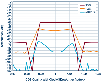
One of the schemes common in converters is correlated double sampling (CDS). See Figure 9 to see how the performance of CDS rejection quality changes with a clock at three different quality levels. The plot shows signals near rejection band. A switched capacitor filter centered at 1 on the x-axis is shown. The center of the plot does not get suppressed by digital filtering and is dependent on the analog switch capacitance filter. A good quality clock is required to preserve a decent rejection level. Even for measuring dc signals, jitter can destroy noise performance by aliasing down unwanted signals that were supposed to be filtered by switched capacitance filters on silicon. The existence of on-board switched capacitance filters may not be explicitly mentioned in data sheets.

Practical Guide, Sources of the Problem, and the Usual Suspects
Now that we have shown a couple of ways that clocks will add to your troubles, it is time to look at techniques to help you build a system that minimizes the amount of jitter.
Clock Signal Reflections
A high quality clock source can have very sharp rise and fall times. This has the benefit of reducing jitter noise at transition time. Unfortunately, with the benefit of sharp edges comes quite stringent demand for proper routing and termination. If the clock line is not terminated properly, the line will suffer from the reflected waves added to the original clock signal. This process is very disruptive and associated jitter levels can easily account for hundreds of picoseconds. In extreme cases, the clock receiver is capable of seeing additional edges that can potentially lead to locked out circuits.


One of the methods that might be counter-intuitive is to slow down the edges with an RC filter, removing high frequency content. One can even use a sinewave as the clock source while waiting for the new PCB with 50 Ω track and termination. While the transition is relatively gradual, and the mark-space ratio can be skewed by hysteresis in digital input, this will reduce the reflection component of jitter.
Power Supply Noise
A digital clock might be routed inside the ADC through a variety of buffers and/or level shifters before the edge is delivered to the sampling switch. If the ADCs have analog supply pins, level shifters are employed and can be sources of jitter. Commonly, the analog side of a chip will have higher voltage devices with longer slewing times, thus jitter sensitivity rises. Some state-of-the-art devices split further analog power supplies between clocked and linear circuits on board.


Decoupling Capacitor: Get the Right One
Jitter sourced by supply noise will be reduced or magnified by the quality of decoupling. Some of the Σ-Δ modulators will have heavy digital activity on the analog and digital sides. This could lead to noncharacteristic spurs with signal or digital data dependent interference. High frequency charge delivery should be limited to a short loop near the device. To accommodate the shortest bondwires, good designs use center pins along the elongated side of the chip. These restrictions are not common problems for amplifiers and low frequency chips, which can have VDD and VSS pins at the corners as in the left side of Figure 12. PCB design should take advantage of those features and keep good quality capacitors near pins.


Clock Dividers and Clock Signal Isolators
Faster clocks have less jitter, so if power constraints allow it, the use of dividers externally or internally to deliver a desired sampling clock can improve things. When designing a system with isolators, review their pulse widths. If there is a poor mark-space ratio, the skew can interfere with analog performance and, in extreme situations, can lock up the digital side of an IC. In precision ADCs, you might not need an optical fiber clock, but using higher frequencies can provide your final bit of performance. In Figure 14, AD9573 uses 2.5 GHz internally only to provide clean 33 MHz and 100 MHz for the same reasons. If there is no need for precise synchronisation between ADCs, the crystal circuit can be very robust with single-digit ps jitter. For precision ADCs, the crystal amplifier translates to better than 22-bits of performance at a 100 kHz input. This performance is hard to beat and explains why XTAL oscillators are here to stay for the foreseeable future.


Crosstalk From Other Signal Sources
Another source of jitter is related to clock disturbances originating in external lines. If the clock source is incorrectly routed near signals capable of coupling, it can have devastating effects on performance. If the interferer is unrelated to ADC operation—and random—it will add to your jitter budget rather gracefully. If the clock is polluted with ADC-related digital signals, one will observe spur. For slave ADCs, CLK lines and SPI lines can be independent clocks, but this can cause problems at frequencies defined in Equation 9 and aliased back to the first Nyqist zone.

It is advisable to use frequency-locked SPI and MCLK sources. Even with this precaution, SPI and MCLK can have spurs associated with the pulse duty cycle of a given clock. For example, if ADC is decimating by 128 and SPI reads only 24 bits, this introduces some risk of creating beat frequency relating to specific 1/(24t) and 1/(104t) measurements. Therefore, you should keep MCLK away from locked SPI lines, as well as data lines.
Interface and Other Clocks
In Figure 15, a variety of timing periods are marked, which can easily disturb SFDR or contribute to jitter. When SPI communications are not frequency locked to MCLK, spurs can occur. Mastery of layout techniques is your biggest asset in mitigating this problem. Frequencies present themselves as aliased down interferers, but also as beat frequencies and intermodulation products. For example, if the SPI is run at 16.01 MHz and the MCLK is at 16 MHz, one could expect spur at 10 kHz.
Outside of good layout, another way of reducing spurs is to move them outside the band of interest. If MCLK and SPI can be frequency locked, a lot of disturbances can be avoided. Even then there is still the problem of idling periods in SPI, contributing to how busy grounds are, which can still cause disturbance. You can use interface features to your advantage. Interface features in ADCs can offer status bytes or cyclic redundancy checks (CRCs). This may provide a great way to suppress spurs with the added benefit of those functions. Idle clocks—and even unused CRC bytes—can be beneficial to fill data frames evenly. You might choose to disregard the CRCs and still get the benefit of turning them on. Of course, this means extra power on digital lines (Figure 18).


Conclusion
In 2018, ADI released the AD7768-1, a very high precision ADC with sub-100 μV of offset and flat frequency response all the way to 100 kHz. It has been successfully designed into systems capable of SFDR in excess of 140 dB where jitter has been proven negligible beyond audio bands with full scale input. It contains an on-board RC oscillator capable of providing reference points to debug disturbed clock sources. This internal RC, while not providing low jitter, can offer differentiation methods to uncover spur sources. The ADC implements internal switched capacitance filtering techniques, but also uses a clock divider to relieve pressure on the antialias filter. The internal clock divider ensures consistent performance that enables operation with skewed clocks commonly received from isolators. The supply positions are ideal for limiting external ESR/ESL effects with short internal bonds. Glitch rejection is implemented in clock input pads. Performance sweeps with applications boards show performance indicating jitter in 30 ps rms, which should satisfy the broad spectrum of applications. If you are tasked with measuring 140+ dB of SFDR, AD7768-1 might be your fastest way of getting the measurement at a fraction of the power previously needed with convenient power supply rails.

References
1 Derek Redmayne, Eric Trelewicz, and Alison Smith. Design Note. “Understanding the Effect of Clock Jitter on High Speed ADCs.” Analog Devices, Inc., 2006.
2 B. E. Boser and B. A. Wooley. “The Design of Sigma–Delta Modulation Analog-to-Digital Converters.” IEEE J. Solid-State Circ., pages 1298–1308, December 1988.
3 Steven Harris. “The Effects of Sampling Clock Jitter on Nyquist Sampling Analog-to-Digital Converters, and on Oversampling Delta–Sigma ADCs.” J. Audio Eng. Society, pages 537–542, July/August 1990.
Beex, A. A. and Monique P. Fargues. “Analysis of Clock Jitter in Switched-Capacitor Systems.” IEEE, July 1992.
Cherry, James A. and W. Martin Snelgrove. “Continuous-Time Delta-Sigma Modulators for High Speed A/D Conversion.” Kluwer Academic Publishers, 2002.
Kester, Walt. “Converting Oscillator Phase Noise to Time Jitter.” Analog Devices, Inc., 2009.
Markell, Richard. Application Note. “Take the Mystery Out of the Switched-Capacitor Filter: The System Designer’s Filter Compendium.” Analog Devices, Inc., March 1990.
