AD4130-8
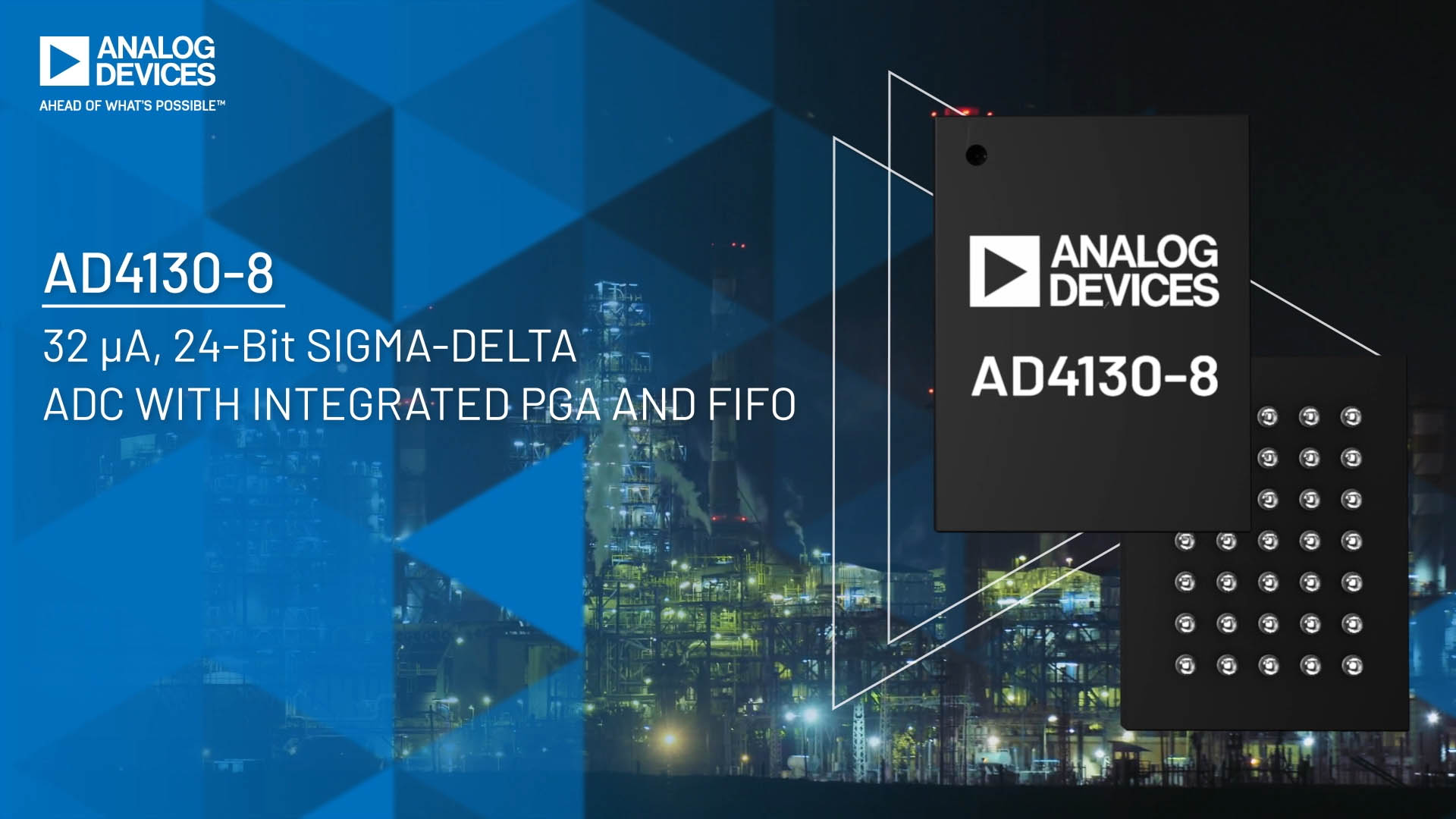
RECOMMENDED FOR NEW DESIGNS32 μA, Ultra Low Power, 24-Bit Sigma-Delta ADC with Integrated PGA and FIFO
- Part Models
- 2
- 1ku List Price
- Starting From $7.28
Overview
- Ultralow current consumption (typical):
- 32 μA: continuous conversion mode (gain = 128)
- 5 μA: duty cycling mode (ratio = 1/16)
- 0.5 μA: standby mode
- 0.1 μA: power-down mode
- Built-in features for system level power savings:
- Current saving duty cycle ratio: 1/4 or 1/16
- Smart sequencer and per channel configuration minimizes host processor load
- Deep embedded FIFO minimizes host processor load (depth of 256 samples)
- Autonomous FIFO interrupt functionality, threshold detection
- Single supply as low as 1.71 V increasing battery length
- RMS noise: 25 nV rms at 1.17 SPS (gain = 128) – 48 nV/√Hz
- Up to 22 noise free bits (gain = 1)
- Output data rate: 1.17 SPS to 2.4 kSPS
- Operates from 1.71 V to 3.6 V single supply or ±1.8 V split supplies
- Band gap reference with 15 ppm/°C maximum drift
- PGA with rail-to-rail analog input
- Adaptable sensor interfacing functionality:
- Matched programmable excitation currents for RTDs
- On-chip bias voltage generator for thermocouples
- Low-side power switch for bridge transducers
- Sensor open wire detection
- Internal temperature sensor and oscillator
- Self and system calibration
- Flexible filter options
- Simultaneous 50 Hz/60 Hz rejection (on selected filter options)
- General-purpose outputs
- Diagnostic functionality
- Crosspoint multiplexed inputs
- 8 differential/16 pseudo differential inputs
- 5 MHz SPI (3-wire or 4-wire)
- Available in 35-ball, 2.74 mm × 3.6 mm WLCSP and 32-lead, 5 mm × 5 mm LFCSP
- Temperature range: −40°C to +105°C (WLCSP), −40°C to +125°C (LFCSP)
- AD4130-8 LFCSP pin compatible with AD7124-8 LFCSP
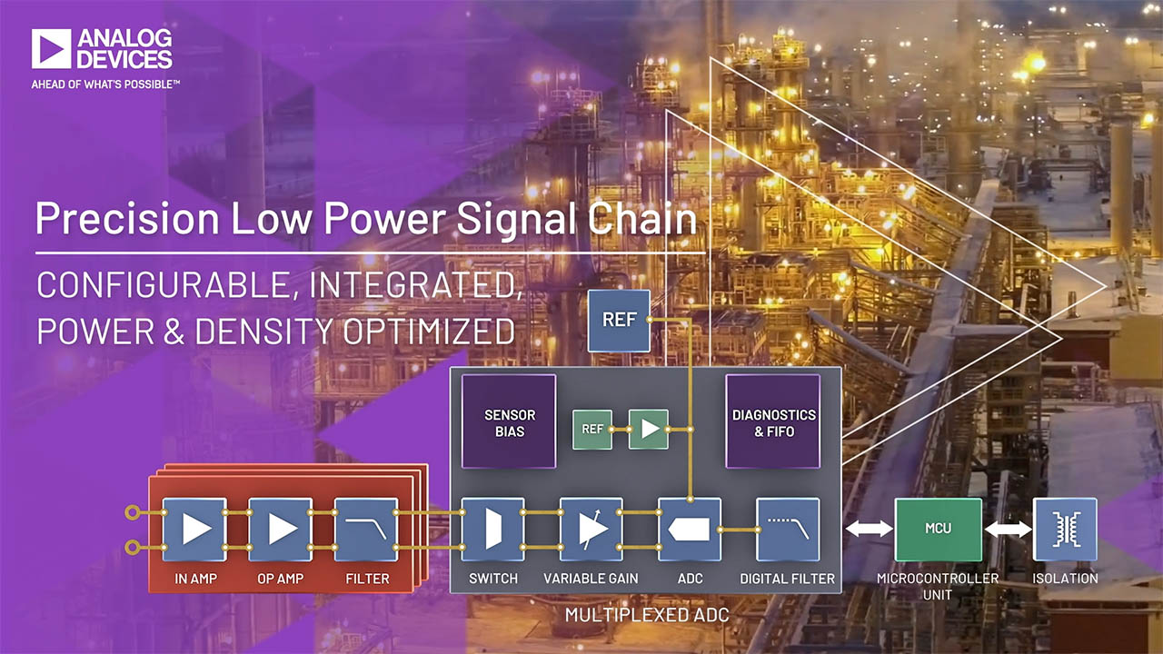
The AD4130-8 is an ultra low power, high precision, measurement solution for low bandwidth battery operated applications. The fully integrated analog front end (AFE) includes a multiplexer for up to 16 single-ended or eight differential inputs, programmable gain amplifier (PGA), 24-bit sigma-delta (Σ-Δ) analog-to-digital converter (ADC), on-chip reference and oscillator, selectable filter options, smart sequencer, sensor biasing and excitation options, diagnostics, and newly added features to improve the battery-operated lifetime (more than 5 years on a coin cell), that is, a first in, first out (FIFO) buffer and duty cycling.
The AD4130-8 allows users to measure low frequency signals with a current consumption of 28.5 μA (gain = 1) and 32.5 μA (gain = 128) while continuously converting, and even lower average currents when using one of the duty cycling options. The AD4130-8 can be configured to have 8 differential inputs or 16 single-ended or pseudo differential inputs, which connect to a crosspoint multiplexer, where any input pair can become a measurement channel input to the PGA and ADC.
The AD4130-8 is designed to allow the user to operate from a single analog supply voltage from 1.71 V to 3.6 V. In battery applications, operation as low as 1.71 V can extend the system lifetime as the AFE can continue its operation, even as the battery voltage dissipates. The digital supply can be separate and range from 1.65 V to 3.6 V.
Together with the reduced current consumption, the integration of an on-chip FIFO buffer can be used in tandem with the smart sequencer, to enable the AD4130-8 to become an autonomous measurement system, which allows the microcontroller to sleep for extended periods.
Intelligent interrupt functionality gives the user a greater confidence in both error detection and safety. The user can enable an interrupt signal to trigger when the samples in the FIFO reach a predefined value or when a user programmable threshold is exceeded.
The following key analog functions are offered on the AD4130-8 to allow simple and effective connection to transducers used for measuring temperature, load, and pressure:
- PGA. Due to the programmable gain (from 1 to 128) and the high input impedance with low input current, the PGA allows direct interfacing to transducers with low output amplitudes like resistive bridges, thermocouples, and resistance temperature detectors (RTDs).
- The capacitive PGA allows full common-mode input range, giving designers greater margin for widely varying input common modes. A wider common-mode input range improves the overall resolution and is highly effective in ratio metric measurements.
- Low drift precision current sources. The IEXC0 and IEXC1 current source can be used to excite 2‑, 3‑, and 4‑wire RTDs. Excitation current output options include 100 nA, 10 μA, 20 μA, 50 μA, 100 μA, 150 μA, and 200 μA.
- The low-side power switch (PDSW) can be used to power down bridge sensors between conversions. The PDSW can be controlled within the sequencer on a per channel basis, allowing optimum timing and energy savings in the overall system. The PDSW can also allow higher powered analog sensors to be used in a low power system.
- Voltage bias for thermocouples (the VBIAS source sets the common-mode voltage of a channel to AVDD/2).
- The smart sequencer allows the conversion of each enabled preconfigured channel in a predetermined order, allowing a mix of transducer, system checks and diagnostic measurements to be interleaved. The sequencer eliminates need for repetitive serial interface communication with the device. Sixteen channels can be configured in the sequence, each of them selecting from eight predefined ADC setups that allow selection of gain, filter type, output data rate, buffering, timing, and reference source.
High levels of integrated front-end functionality coupled with small package options allow smaller end solutions. For example, the AD4130-8 integrates a low thermal drift band gap reference in addition to accepting an external differential reference, which can be internally buffered.
In safety critical applications the AD4130-8 includes diagnostic functionality such as open wire detection via burnout currents, internal temperature sensor, reference detection, and analog input overvoltage and undervoltage detection. Added diagnostics are included on the digital interface like cyclic redundancy check (CRC) and serial interface checks for a robust communication link.
APPLICATIONS
- Smart transmitters
- Wireless battery and harvester powered sensor nodes
- Portable instrumentation
- Temperature measurement: thermocouple, RTD, thermistors
- Pressure measurement: bridge transducers
- Healthcare and wearables
Documentation
Data Sheet 1
User Guide 1
Video 4
Device Drivers 2
Thought Leadership 1
Analog Dialogue 2
Webcast 5
ADI has always placed the highest emphasis on delivering products that meet the maximum levels of quality and reliability. We achieve this by incorporating quality and reliability checks in every scope of product and process design, and in the manufacturing process as well. "Zero defects" for shipped products is always our goal. View our quality and reliability program and certifications for more information.
| Part Model | Pin/Package Drawing | Documentation | CAD Symbols, Footprints, and 3D Models |
|---|---|---|---|
| AD4130-8BCBZ-RL7 | 35-Ball WLCSP (2.70 mm x 3.56mm x 0.50 mm) | ||
| AD4130-8BCPZ-RL7 | 32-Lead LFCSP (5mm x 5mm x 0.75mm w/ EP) |
| Part Models | Product Lifecycle | PCN |
|---|---|---|
|
Jun 26, 2023 - 23_0123 Datasheet correction for AD4130-8 |
||
| AD4130-8BCBZ-RL7 | PRODUCTION | |
This is the most up-to-date revision of the Data Sheet.
Software Resources
Mbed Support 2
Evaluation Software 0
Can't find the software or driver you need?
Hardware Ecosystem
-
Multichannel, Differential Input, 24 Bits, Below 24 kSPS Low Noise, Low Power -
Multichannel, Differential Input, 24 Bits, Below 24 kSPS Low Noise, Fast Settling
| Parts | Product Life Cycle | Description |
|---|---|---|
| Charge Pumps 1 | ||
| LTC1983 | PRODUCTION | 100mA Regulated Charge-Pump Inverters in ThinSOT |
| LDO Linear Regulators 2 | ||
| ADP150 | PRODUCTION | Ultralow Noise, 150 mA CMOS Linear Regulator |
| ADP7182 | RECOMMENDED FOR NEW DESIGNS | –28 V, −200 mA, Low Noise, Linear Regulator |
| Microcontrollers 3 | ||
| MAX32670 | PRODUCTION | High-Reliability, Ultralow-Power Microcontroller Powered by Arm Cortex-M4 Processor with FPU for Industrial and IoT |
| MAX32655 | RECOMMENDED FOR NEW DESIGNS | Low-Power, Arm Cortex-M4 Processor with FPU-Based Microcontroller and Bluetooth 5.2 |
| MAX32663A | PRODUCTION | Ultra-Low Power ECG Biometric Sensor Hub |
| Voltage References 2 | ||
| ADR3625 | RECOMMENDED FOR NEW DESIGNS | Precision, Micropower, High Current Output Voltage Reference |
| ADR391 | PRODUCTION | 2.5V Micropower, Low Noise Precision Voltage Reference with Shutdown |
Tools & Simulations
LTspice
Models for the following parts are available in LTspice:
- AD4130-8
Design Tool 1
ADI Circuit Explorer™
ADI Circuit Explorer™ uses AI to interpret natural language prompts and search a database of validated analog circuit designs, helping you quickly find the best match for your needs.
Open ToolSignal Chain Designer
Signal Chain Designer is a web-based tool designed to create and simulate complex precision signal chains. See your circuit’s performance before you commit to your PCB: transfer function, noise, power consumption, input range, and DC error. Quickly experiment with different parts and architectures. Signal chains can be exported to LTspice for further analysis.
Open ToolLTspice® is a powerful, fast and free simulation software, schematic capture and waveform viewer with enhancements and models for improving the simulation of analog circuits.
Evaluation Kits
Latest Discussions
No discussions on AD4130-8 yet. Have something to say?
Start a Discussion on EngineerZone®


