RF & Microwave

- Beamformers & Vector Modulators
- Frequency Dividers & Multipliers
- Mixed Signal Front Ends (MxFE)
- Modulators & Demodulators
- Oscillators
- Phase Shifters
- PLL Synthesizers
- RF ADCs
- RF Amplifiers
- RF Analog Receivers & Transmitters
- RF Attenuators
- RF DACs & DDS
- RF Mixers
- RF Power Detectors
- RF Switches
- Software Defined Radio
- Tunable Filters & RF Limiters
- Voltage to Frequency Converters
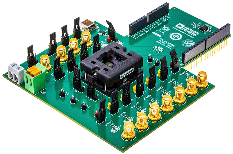
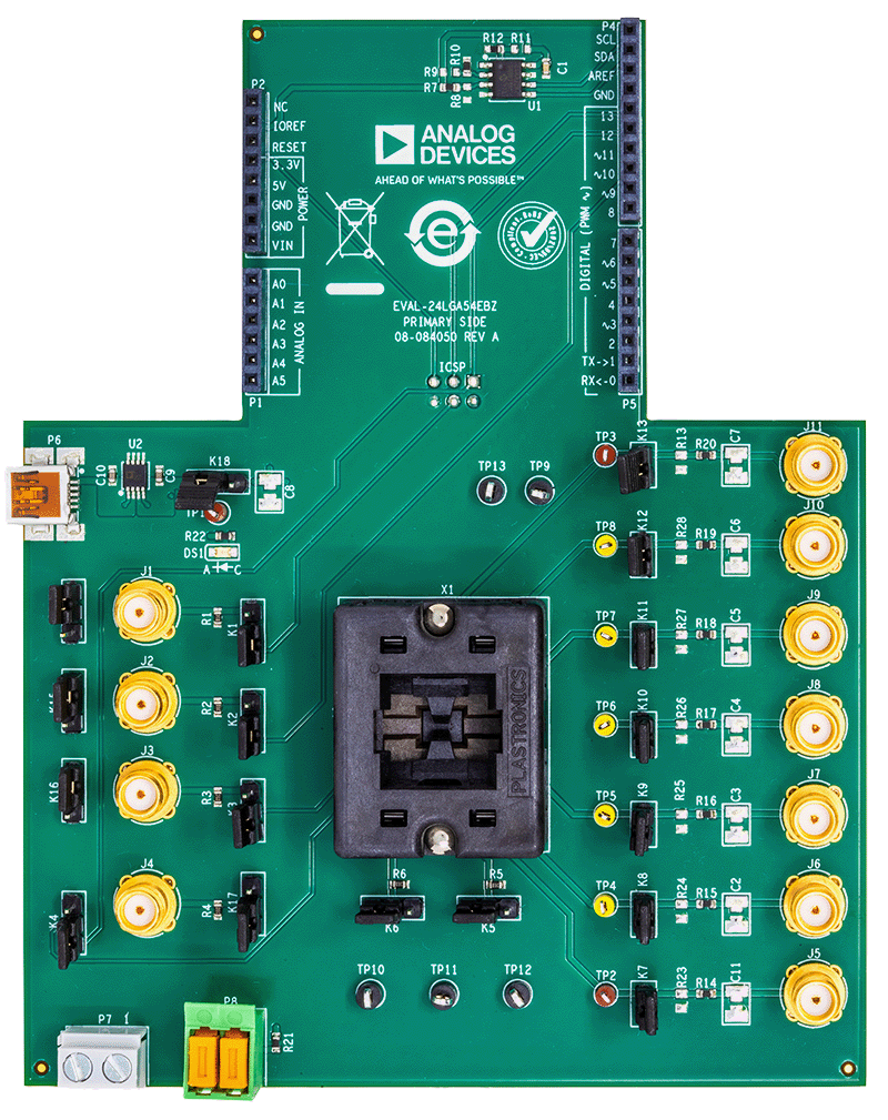
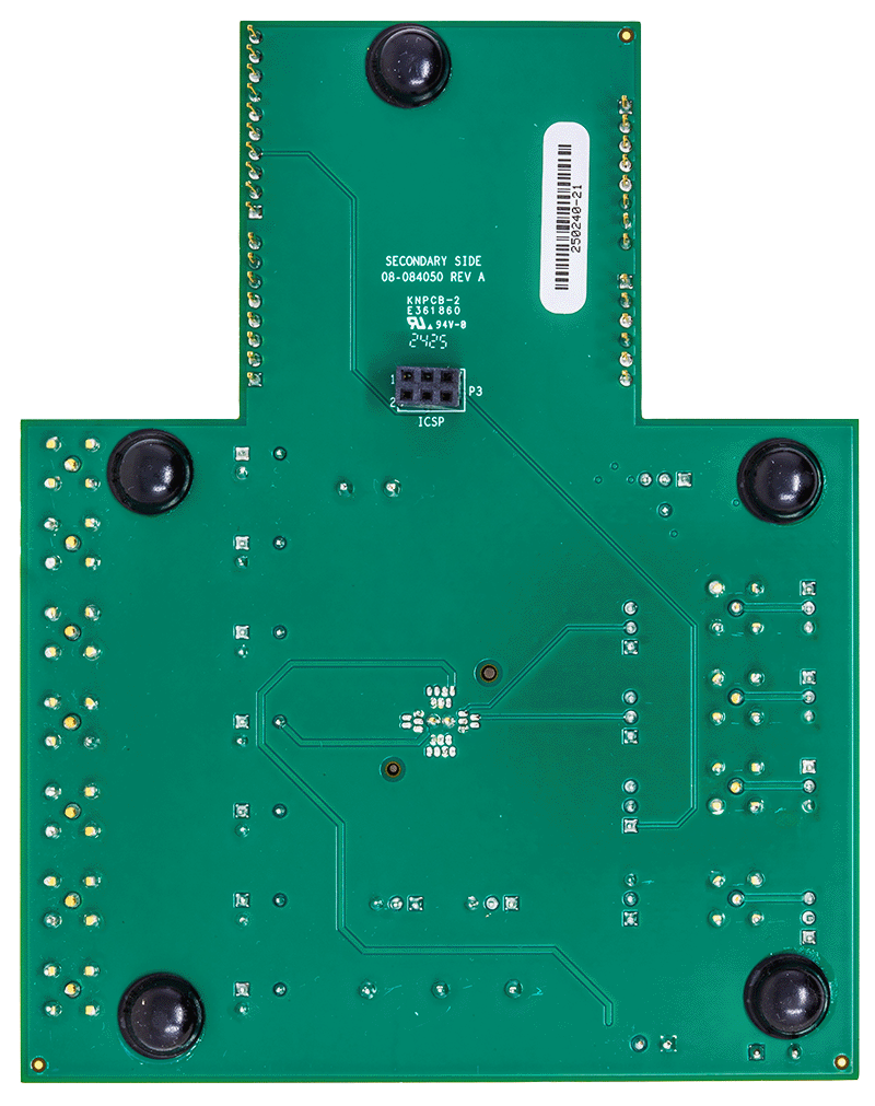
ADGM1304