Temperature Sensing
Temperature is the world’s most widely measured physical phenomenon. There are four main temperature sensor technologies, each with its own signal conditioning challenges.
- Thermocouples: small, rugged, and inexpensive, thermocouples have a wide temperature range (–270°C to +1800°C), but they require complicated signal conditioning and linearization.
- Thermistors: inexpensive, but they have a limited temperature range (typically –40°C to 150°C ), are highly nonlinear, and require significant signal conditioning.
- RTDs: accurate, stable, and have a wide temperature range. RTDs require precision signal conditioning to take full advantage of their accuracy. The most accurate RTDs are built with platinum and are more expensive than other temperature sensors.
- Silicon-Based Temperature Measurement: linear, stable, and easy to use silicon-based temperature sensors are best when measuring a narrower temperature range (–55°C to +150°C).
- Digital Sensors: linear, stable, and easy to use digital sensors offer the highest accuracy with breakthrough performance over a wide industrial temperature range (–20°C to +105°C).
Whichever temperature sensor type you choose, ADI has a wealth of signal chains, integrated solutions, and discrete technologies to jump start your design.
Signal Chains
(5)
Interactive Signal Chains

Reference Designs
CN0384

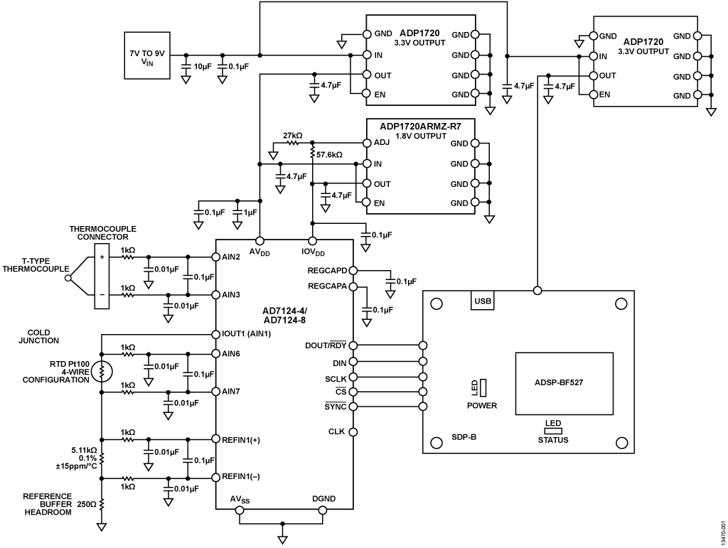
The circuit shown in Figure 1 is an integrated thermocouple measurement system based on the AD7124-4/AD7124-8 low power, low noise, 24-bit, Σ-Δ analog-to-digital converter (ADC), optimized for high precision measurement applications. Thermocouple measurements using this system show an overall system accuracy of ±1°C over a measurement temperature range of −50°C to +200°C . Typical noise free code resolution of the system is approximately 15 bits.

The AD7124-4 can be configured for 4 differential or 7 pseudo differential input channels, while the AD7124-8 can be configured for 8 differential or 15 pseudo differential channels. The on-chip low noise programmable gain array (PGA) ensures that signals of small amplitude can be interfaced directly to the ADC.
The AD7124-4/AD7124-8 establishes the highest degree of signal chain integration, which includes programmable low drift excitation current sources, bias voltage generator, and internal reference. Therefore, the design of a thermocouple system is simplified when the AD7124-4/AD7124-8 is used because most of the required system building blocks are included on-chip.
The AD7124-4/AD7124-8 gives the user the flexibility to employ one of three integrated power modes, where the current consumption, range of output data rates, and rms noise are tailored with the power mode selected. The current consumed by the AD7124-4/AD7124-8 is only 255 μA in low power mode and 930 μA in full power mode. The power options make the device suitable for non-power critical applications, such as input/output modules, and also for low power applications, such as loop-powered smart transmitters where the complete transmitter must consume less than 4 mA.
The device also has a power-down option. In power-down mode, the complete ADC along with its auxiliary functions are powered down so that the device consumes 1 μA typical. The AD7124-4/AD7124-8 also has extensive diagnostic functionality integrated as part of its comprehensive feature set.
Applicable Parts
Applications
CN0354

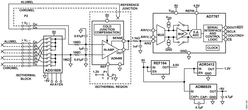
The circuit shown in Figure 1 is a flexible, 4-channel, low power thermocouple measurement circuit with an overall power consumption of less than 8 mW. The circuit has a multiplexed front end, followed by an instrumentation amplifier that performs cold junction compensation (0°C to 50°C) and converts the thermocouple output to a voltage with a precise scale factor of 5 mV/°C. The error is less than 2°C, over a measurement range of −25°C to +400°C, and is primarily due to the thermocouple nonlinearity. A nonlinearity correction algorithm reduces the error to less than 0.5°C over a 900°C measurement range. Noise free resolution is less than 0.1°C.
The signal is then digitized by a 24-bit Σ-Δ ADC, and the digital value is provided on an SPI serial interface. With the PMOD form factor for rapid prototyping, the design requires minimal PC board area and is ideal for applications that require precise thermocouple temperature measurements.

Applicable Parts
AD7787
Low Power, 2-Channel 24-Bit Sigma-Delta ADC
AD8495
Full K-Type Range 0° to 50° Thermocouple Amplifier w/Cold Junction Compensation
ADG1609
4.5 Ω RON, 4-Channel ±5 V,+12 V, +5 V, and +3.3 V Multiplexer
ADM8829
Switched Capacitor Voltage Inverter
ADR3412
Micro-Power, High-Accuracy 1.2V Voltage Reference.
REF194
4.5V Precision Micropower, Low Dropout, Low Voltage Reference
Applications
CN0383

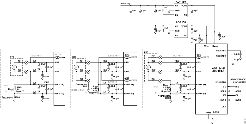
The circuit shown in Figure 1 is an integrated 2-wire, 3-wire, or 4-wire resistance temperature detector (RTD) system based on the AD7124-4/AD7124-8 low power, low noise, 24-bit Σ-Δ analog-to-digital converter (ADC) optimized for high precision measurement applications.

This circuit note uses a Class B Pt100 RTD sensor with an accuracy of ±0.3°C at 0°C but it can support other classes such as Class A, Class AA, 1/3 DIN, or 1/10 DIN that are higher accuracy RTDs. This circuit also has provision for Pt1000 RTDs that are useful in low power applications.
The AD7124-4/AD7124-8 can achieve high resolution, low nonlinearity, and low noise performance as well as high 50 Hz and 60 Hz rejection, suitable for industrial RTD systems. The typical peak to peak resolution of the system is 0.0043°C (17.9 bits) for full power mode, sinc4 filter selected, at an output data rate of 50 SPS, and 0.0092°C (16.8 bits) for low power mode, post filter selected, at an output data rate of 25 SPS. These settings show that the system accuracy is significantly better than the sensor accuracy.
The AD7124-4/AD7124-8 integrate several important system building blocks required to support RTD measurements. Functions, including programmable excitation current sources and a programmable gain amplifier (PGA), excite and gain the RTD, respectively, which allows direct interfacing with the sensor and simplifies the design while reducing cost and power consumption.
Several options of the on-chip digital filtering and three integrated power modes, where the current consumption, range of output data rates, settling time, and rms noise are optimized, provide application flexibility. The current consumed in low power mode is only 255 μA and in full power mode is 930 μA. In power-down mode, the complete ADC along with its auxiliary functions are powered down so that the AD7124-4/AD7124-8 consume 1 μA typical. The power options make the AD7124-4/AD7124-8 suitable for nonpower critical applications, such as input modules, and also for low power applications, such as loop-powered smart transmitters where the complete transmitter must consume less than 4 mA.
The AD7124-4/AD7124-8 also have extensive diagnostic functionality integrated as part of its comprehensive feature set. This functionality can be used to check that the voltage level on the analog pins are within the specified operating range. These devices also include a cyclic redundancy check (CRC) on the serial peripheral interface (SPI) bus and signal chain checks, which leads to a more robust solution. These diagnostics reduce the need for external components to implement diagnostics, resulting in a smaller solution size, reduced design cycle times, and cost savings.
Applicable Parts
Applications
CN0172

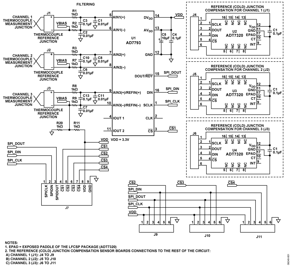
The function of the circuit shown in Figure 1 is to provide a high accuracy multichannel thermocouple measurement solution. Achieving a precision thermocouple measurement requires a signal chain of precision components that amplifies the small thermocouple voltage, reduces noise, corrects nonlinearity, and provides accurate reference junction compensation (commonly referred to as cold junction compensation). This circuit addresses all these challenges for measuring thermocouple temperature with better than ±0.25°C accuracy.
The circuit shown in Figure 1 shows how three K type thermocouples are connected to the AD7793 precision 24-bit sigma-delta (Σ-Δ) analog-to-digital converter (ADC) to measure the thermocouple voltage. Because the thermocouple is a differential device rather than an absolute temperature measurement device, the reference junction temperature must be known to get an accurate absolute temperature reading. This process is known as reference junction compensation, commonly referred to as cold junction compensation. In this circuit, the ADT7320 precision 16-bit digital temperature sensor is used for the cold junction reference measurement and provides the required accuracy.
This type of application is popular where a cost-effective, accurate temperature measurement is required over the wide temperature ranges offered by thermocouples.

Applicable Parts
Applications
CN0376

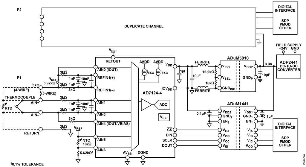
The circuit shown in Figure 1 provides a dual-channel, channel-to-channel isolated, thermocouple or RTD input suitable for programmable logic controllers (PLC) and distributed control systems (DCS). The highly integrated design utilizes a low power, 24-bit, Σ-Δ analog-to-digital converter (ADC) with a rich analog and digital feature set that requires no additional signal conditioning ICs.
Each channel can accept either a thermocouple or a RTD input. The entire circuit is powered from a standard 24 V bus supply. Each channel measures only 27 mm × 50 mm.

Applicable Parts
AD7124-4
4-Channel, Low Noise, Low Power, 24-Bit, Sigma-Delta ADC with PGA and Reference
AD7124-8
8-Channel, Low Noise, Low Power, 24-Bit, Sigma-Delta ADC with PGA and Reference
ADUM5010
2.5kV rms Isolated DC/DC Converter
ADUM1441
Micropower Quad-Channel Digital Isolator, Default High (3/1 Channel Directionality)
ADP2441
36 V,1 A, Synchronous, Step-Down DC-DC Regulator
Applications
Featured Products
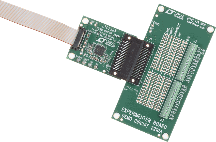
LTC2983

The LTC2983 measures a wide variety of temperature sensors and digitally outputs the result, in °C or °F, with 0.1°C accuracy and 0.001°C resolution. The LTC2983 can measure the temperature of virtually all standard (type B, E, J, K, N, S, R, T) or custom thermocouples, automatically compensate for cold junction temperatures and linearize the results. The device can also measure temperature with standard 2-, 3- or 4-wire RTDs, thermistors and diodes. It has 20 reconfigurable analog inputs enabling many sensor connections and configuration options. The LTC2983 includes excitation current sources and fault detection circuitry appropriate for each type of temperature sensor.
The LTC2983 allows direct interfacing to ground referenced sensors without the need for level shifters, negative supply voltages, or external amplifiers. All signals are buffered and simultaneously digitized with three high accuracy, 24-bit ΔΣ ADCs, driven by an internal 10ppm/°C (maximum) reference.
Applications
- Direct Thermocouple Measurements
- Direct RTD Measurements
- Direct Thermistor Measurements
- Custom Sensor Applications
Applications
Instrumentation & Measurement
ADUCM360

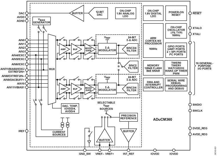
The ADuCM360/ADuCM361 contain an on-chip 32 kHz oscillator and an internal 16 MHz high frequency oscillator. The high frequency oscillator is routed through a programmable clock divider from which the operating frequency of the processor core clock is generated. The maximum core clock speed is 16 MHz; this speed is not limited by operating voltage or temperature.
The microcontroller core is a low power ARM Cortex-M3 processor, a 32-bit RISC machine that offers up to 20 MIPS peak performance. The Cortex-M3 processor incorporates a flexible, 11-channel DMA controller that supports all wired communica-tion peripherals (SPI, UART, and I2C). Also integrated on chip are 128 kB of nonvolatile Flash/EE memory and 8 kB of SRAM.
The analog subsystem consists of dual ADCs, each connected to a flexible input mux. Both ADCs can operate in fully differential and single-ended modes. Other on-chip ADC features include dual programmable excitation current sources, diagnostic current sources, and a bias voltage generator of AVDD_REG/2 (900 mV) to set the common-mode voltage of an input channel. A low-side internal ground switch is provided to allow power-down of an external circuit (for example, a bridge circuit) between conversions.
The ADCs contain two parallel filters: a sinc3 or sinc4 filter in parallel with a sinc2 filter. The sinc3 or sinc4 filter is used for precision measurements. The sinc2 filter is used for fast measure-ments and for the detection of step changes in the input signal.
The devices contain a low noise, low drift internal band gap ref-erence, but they can be configured to accept one or two external reference sources in ratiometric measurement configurations. An option to buffer the external reference inputs is provided on chip. A single-channel buffered voltage output DAC is also provided on chip.
The ADuCM360/ADuCM361 integrate a range of on-chip peripherals, which can be configured under microcontroller software control as required in the application. The peripherals include UART, I2C, and dual SPI serial I/O communication controllers; a 19-pin GPIO port; two general-purpose timers; a wake-up timer; and a system watchdog timer. A 16-bit PWM controller with six output channels is also provided.
The ADuCM360/ADuCM361 are specifically designed to operate in battery-powered applications where low power operation is critical. The microcontroller core can be configured in a normal operating mode that consumes 290 μA/MHz (including flash/ SRAM IDD). An overall system current consumption of 1 mA can be achieved with both ADCs on (input buffers off), PGA gain of 4, one SPI port on, and all timers on.
The ADuCM360/ADuCM361 can be configured in a number of low power operating modes under direct program control, including a hibernate mode (internal wake-up timer active) that consumes only 4 μA. In hibernate mode, peripherals such as external interrupts or the internal wake-up timer can wake up the device. This mode allows the part to operate with ultralow power and still respond to asynchronous external or periodic events.
APPLICATIONS
- Industrial automation and process control
- Intelligent precision sensing systems
- 4 mA to 20 mA loop-powered smart sensor systems
- Medical devices, patient monitoring
Applications
ADT7420

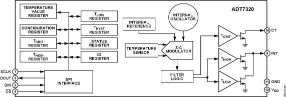
The ADT7420 is a high accuracy digital temperature sensor offering breakthrough performance over a wide industrial range, housed in a 4 mm × 4 mm LFCSP package. It contains an internal band gap reference, a temperature sensor, and a 16-bit ADC to monitor and digitize the temperature to 0.0078°C resolution. The ADC resolution, by default, is set to 13 bits (0.0625°C). The ADC resolution is a user programmable mode that can be changed through the serial interface.
The ADT7420 is guaranteed to operate over supply voltages from 2.7 V to 5.5 V. Operating at 3.3 V, the average supply current is typically 210 μA. The ADT7420 has a shutdown mode that powers down the device and offers a shutdown current of typically 2.0 μA at 3.3 V. The ADT7420 is rated for operation over the −40°C to +150°C temperature range.
Pin A0 and Pin A1 are available for address selection, giving the ADT7420 four possible I2C addresses. The CT pin is an open-drain output that becomes active when the temperature exceeds a programmable critical temperature limit. The INT pin is also an open-drain output that becomes active when the temperature exceeds a programmable limit. The INT pin and CT pin can operate in comparator and interrupt event modes.
Product Highlights
- Ease of use, no calibration or correction required by the user.
- Low power consumption.
- Excellent long-term stability and reliability.
- High accuracy for industrial, instrumentation, and medical applications.
- Packaged in a 16-lead, 4 mm × 4 mm LFCSP RoHS-compliant package.
Applications
- RTD and thermistor replacement
- Thermocouple cold junction compensation
- Medical equipment
- Industrial control and test
- Food transportation and storage
- Environmental monitoring and HVAC
- Laser diode temperature control
Applications
ADT7320

The ADT7320 is a high accuracy digital temperature sensor that offers breakthrough performance over a wide industrial temperature range, housed in a 4 mm × 4 mm LFCSP package. It contains an internal band gap reference, a temperature sensor, and a 16-bit analog-to-digital converter (ADC) to monitor and digitize the temperature to a resolution of 0.0078°C. The ADC resolution, by default, is set to 13 bits (0.0625°C). The ADC resolution is a user programmable mode that can be changed through the serial interface.
The ADT7320 is guaranteed to operate over supply voltages from 2.7 V to 5.5 V. Operating at 3.3 V, the average supply current is typically 210 μA. The ADT7320 has a shutdown mode that powers down the device and offers a shutdown current of typically 2.0 μA at 3.3 V. The ADT7320 is rated for operation over the −40°C to +150°C temperature range.
The CT pin is an open-drain output that becomes active when the temperature exceeds a programmable critical temperature limit. The INT pin is also an open-drain output that becomes active when the temperature exceeds a programmable limit. The INT pin and CT pin can operate in either comparator or interrupt mode.
PRODUCT HIGHLIGHTS
- Ease of use, no calibration or correction required by the user.
- Low power consumption.
- Excellent long term stability and reliability.
- High accuracy for industrial, instrumentation, and medical applications.
- Packaged in a 16-lead RoHS-compliant, 4 mm x 4 mm LFCSP package.
APPLICATIONS
- RTD and thermistor replacement
- Thermocouple cold junction compensation
- Medical equipment
- Industrial controls and test
- Food transportation and storage
- Environmental monitoring and HVAC
- Laser diode temperature controls
Applications
Intelligent Buildings
- Building Automation Systems
- Building Sustainability
- Environmental Monitoring Solutions
- Building Utilities
- HVAC Systems Technologies
AD7124-4

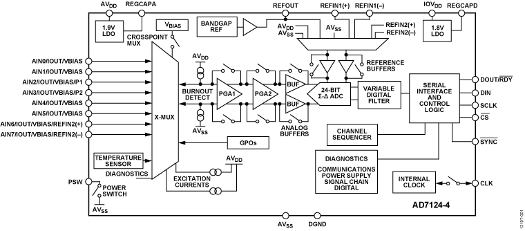
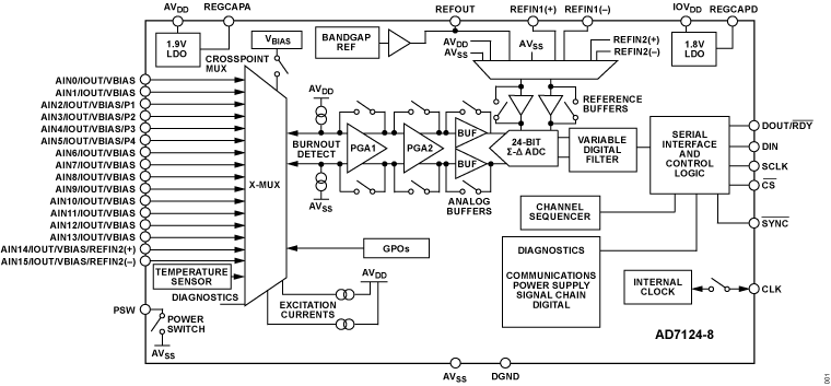
The AD7124-4 is a low power, low noise, completely integrated analog front end for high precision measurement applications. The device contains a low noise, 24-bit Σ-Δ analog-to-digital converter (ADC), and can be configured to have 4 differential inputs or 7 single-ended or pseudo differential inputs. The onchip low gain stage ensures that signals of small amplitude can be interfaced directly to the ADC.
One of the major advantages of the AD7124-4 is that it gives the user the flexibility to employ one of three integrated power modes. The current consumption, range of output data rates, and rms noise can be tailored with the power mode selected. The device also offers a multitude of filter options, ensuring that the user has the highest degree of flexibility.
The AD7124-4 can achieve simultaneous 50 Hz and 60 Hz rejection when operating at an output data rate of 25 SPS (single cycle settling), with rejection in excess of 80 dB achieved at lower output data rates.
The AD7124-4 establishes the highest degree of signal chain integration. The device contains a precision, low noise, low drift internal band gap reference, and also accepts an external differential reference, which can be internally buffered. Other key integrated features include programmable low drift excitation current sources, burnout currents, and a bias voltage generator, which sets the common-mode voltage of a channel to AVDD/2. The low-side power switch enables the user to power down bridge sensors between conversions, ensuring the absolute minimal power consumption of the system. The device also allows the user the option of operating with either an internal clock or an external clock.
The integrated channel sequencer allows several channels to be enabled simultaneously, and the AD7124-4 sequentially converts on each enabled channel, simplifying communication with the device. As many as 16 channels can be enabled at any time; a channel being defined as an analog input or a diagnostic such as a power supply check or a reference check. This unique feature allows diagnostics to be interleaved with conversions.
The AD7124-4 also supports per channel configuration. The device allows eight configurations or setups. Each configuration consists of gain, filter type, output data rate, buffering, and reference source. The user can assign any of these setups on a channel by channel basis.
The AD7124-4 also has extensive diagnostic functionality integrated as part of its comprehensive feature set. These diagnostics include a cyclic redundancy check (CRC), signal chain checks, and serial interface checks, which lead to a more robust solution. These diagnostics reduce the need for external components to implement diagnostics, resulting in reduced board space needs, reduced design cycle times, and cost savings. The failure modes effects and diagnostic analysis (FMEDA) of a typical application has shown a safe failure fraction (SFF) greater than 90% according to IEC 61508.
The device operates with a single analog power supply from 2.7 V to 3.6 V or a dual 1.8 V power supply. The digital supply has a range of 1.65 V to 3.6 V. It is specified for a temperature range of −40°C to +105°C. The AD7124-4 is housed in a 32-lead LFCSP package or a 24-lead TSSOP package.
Applications
- Temperature measurement
- Pressure measurement
- Industrial process control
- Instrumentation Smart transmitters
- Smart transmitters
Applications
Intelligent Buildings
- Building Automation Systems
- Building Automation Controllers and Networks
- Building Utilities
- Building Safety and Security Solutions
AD7124-8

The AD7124-8 is a low power, low noise, completely integrated analog front end for high precision measurement applications. The AD7124-8 W grade is AEC-Q100 qualified for automotive applications. The device contains a low noise, 24-bit Σ-Δ analog-to-digital converter (ADC), and can be configured to have 8 differential inputs or 15 single-ended or pseudo differential inputs. The on-chip low gain stage ensures that signals of small amplitude can be interfaced directly to the ADC.
One of the major advantages of the AD7124-8 is that it gives the user the flexibility to employ one of three integrated power modes. The current consumption, range of output data rates, and rms noise can be tailored with the power mode selected. The device also offers a multitude of filter options, ensuring that the user has the highest degree of flexibility.
The AD7124-8 can achieve simultaneous 50 Hz and 60 Hz rejection when operating at an output data rate of 25 SPS (single cycle settling), with rejection in excess of 80 dB achieved at lower output data rates.
The AD7124-8 establishes the highest degree of signal chain integration. The device contains a precision, low noise, low drift internal band gap reference and accepts an external differential reference, which can be internally buffered. Other key integrated features include programmable low drift excitation current sources, burnout currents, and a bias voltage generator, which sets the common-mode voltage of a channel to AVDD/2. The low-side power switch enables the user to power down bridge sensors between conversions, ensuring the absolute minimal power consumption of the system. The device also allows the user the option of operating with either an internal clock or an external clock.
The integrated channel sequencer allows several channels to be enabled simultaneously, and the AD7124-8 sequentially converts on each enabled channel, simplifying communication with the device. As many as 16 channels can be enabled at any time, a channel being defined as an analog input or a diagnostic such as a power supply check or a reference check. This unique feature allows diagnostics to be interleaved with conversions. The AD7124-8 also supports per channel configuration. The device allows eight configurations or setups. Each configuration consists of gain, filter type, output data rate, buffering, and reference source. The user can assign any of these setups on a channel by channel basis.
The AD7124-8 also has extensive diagnostic functionality integrated as part of its comprehensive feature set. These diagnostics include a cyclic redundancy check (CRC), signal chain checks, and serial interface checks, which lead to a more robust solution. These diagnostics reduce the need for external components to implement diagnostics, resulting in reduced board space needs, reduced design cycle times, and cost savings. The failure modes effects and diagnostic analysis (FMEDA) of a typical application has shown a safe failure fraction (SFF) greater than 90% according to IEC 61508.
The device operates with a single analog power supply from 2.7 V to 3.6 V or a dual 1.8 V power supply. The digital supply has a range of 1.65 V to 3.6 V. It is specified for a temperature range of −40°C to +125°C. The AD7124-8 is housed in a 32-lead LFCSP package.
APPLICATIONS
- Temperature measurement
- Pressure measurement
- Industrial process control
- Instrumentation
- Smart transmitters
Applications
Intelligent Buildings
- Building Automation Systems
- Building Automation Controllers and Networks
- Building Safety and Security Solutions
AD8226

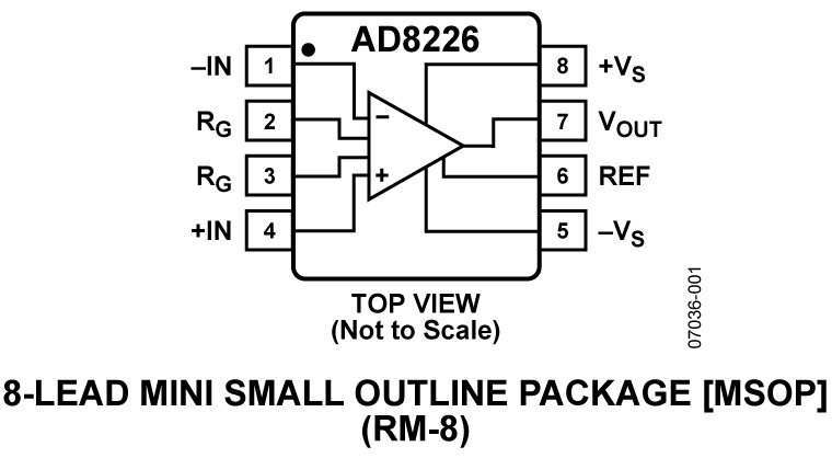
The AD8226 is a low cost, wide supply range instrumentation amplifier that requires only one external resistor to set any gain between 1 and 1000.
The AD8226 is designed to work with a variety of signal voltages. A wide input range and rail-to-rail output allow the signal to make full use of the supply rails. Because the input range also includes the ability to go below the negative supply, small signals near ground can be amplified without requiring dual supplies. The AD8226 operates on supplies ranging from ±1.35 V to ±18 V for dual supplies and 2.2 V to 36 V for single supply.
The robust AD8226 inputs are designed to connect to real-world sensors. In addition to its wide operating range, the AD8226 can handle voltages beyond the rails. For example, with a ±5 V supply, the part is guaranteed to withstand ±35 V at the input with no damage. Minimum as well as maximum input bias currents are specified to facilitate open wire detection.
The AD8226 is perfect for multichannel, space-constrained industrial applications. Unlike other low cost, low power instrumentation amplifiers, the AD8226 is designed with a minimum gain of 1 and can easily handle ±10 V signals. With its MSOP package and 125°C temperature rating, the AD8226 thrives in tightly packed, zero airflow designs.
The AD8226 is available in 8-lead MSOP and SOIC packages, and is fully specified for −40°C to +125°C operation.
For a device with a similar package and performance as the AD8226 but with gain settable from 5 to 1000, consider using the AD8227.
Applications
Applications
AD7175-2

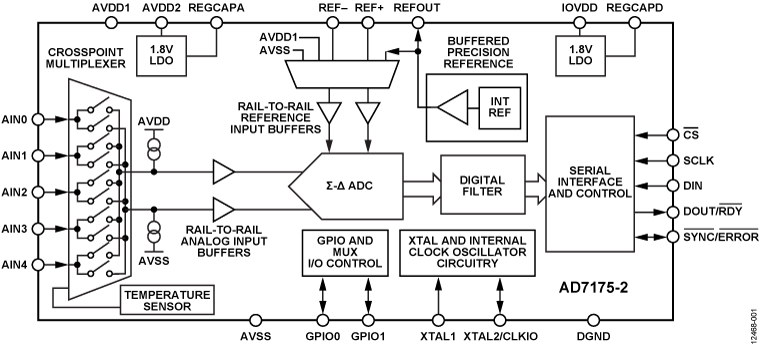
The AD7175-2 is a low noise, fast settling, multiplexed, 2-/4- channel (fully/pseudo differential) Σ-Δ analog-to-digital converter (ADC) for low bandwidth inputs. It has a maximum channel scan rate of 50 kSPS (20 µs) for fully settled data. The output data rates range from 5 SPS to 250 kSPS.
The AD7175-2 integrates key analog and digital signal conditioning blocks to allow users to configure an individual setup for each analog input channel in use. Each feature can be user selected on a per channel basis. Integrated true rail-to-rail buffers on the analog inputs and external reference inputs provide easy to drive high impedance inputs. The precision 2.5 V low drift (2 ppm/°C) band gap internal reference (with output reference buffer) adds embedded functionality to reduce external component count.
The digital filter allows simultaneous 50 Hz/60 Hz rejection at 27.27 SPS output data rate. The user can switch between different filter options according to the demands of each channel in the application. The ADC automatically switches through each selected channel. Further digital processing functions include offset and gain calibration registers, configurable on a per channel basis.
The device operates with a 5 V AVDD1, or ±2.5 V AVDD1/AVSS, and 2 V to 5 V AVDD2 and IOVDD supplies. The specified operating temperature range is −40°C to +105°C. The AD7175-2 is in a 24-lead TSSOP package.
Applications
- Process control: PLC/DCS modules
- Temperature and pressure measurement
- Medical and scientific multichannel instrumentation
- Chromatography
Applications
Intelligent Buildings
- Building Utilities
AD7175-8

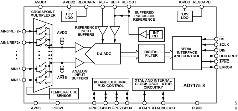
The AD7175-8 is a low noise, fast settling, multiplexed, 8-/16- channel (fully/pseudo differential) Σ-Δ analog-to-digital converter (ADC) for low bandwidth inputs. It has a maximum channel scan rate of 50 kSPS (20 ìs) for fully settled data. The output data rates range from 5 SPS to 250 kSPS.
The AD7175-8 integrates key analog and digital signal condition-ing blocks to allow users to configure an individual setup for each analog input channel in use. Each feature can be user selected on a per channel basis. Integrated true rail-to-rail buffers on the analog inputs and external reference inputs provide easy to drive high impedance inputs. The precision 2.5 V low drift (2 ppm/°C) band gap internal reference (with output reference buffer) adds embedded functionality to reduce external component count.
The digital filter allows simultaneous 50 Hz and 60 Hz rejection at a 27.27 SPS output data rate. The user can switch between different filter options according to the demands of each channel in the application. The ADC automatically switches through each selected channel. Further digital processing functions include offset and gain calibration registers, configurable on a per channel basis.
The device operates with a 5 V AVDD1 . AVSS supply, or with ±2.5 V AVDD1/AVSS, and 2.5 V to 5 V AVDD2 and IOVDD supplies. The specified operating temperature range is .40°C to +105°C. The AD7175-8 is available in a 40-lead LFCSP package.
APPLICATIONS
- Process control: PLC/DCS modules
Temperature and pressure measurement - Medical and scientific multichannel instrumentation
- Chromatography
Applications
Intelligent Buildings
- Building Utilities
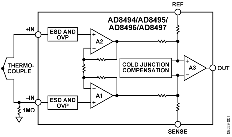
AD8494

The AD8494/AD8495/AD8496/AD8497 are precision instrumentation amplifiers with thermocouple cold junction compensators on an integrated circuit. They produce a high level (5 mV/°C) output directly from a thermocouple signal by combining an ice point reference with a precalibrated amplifier. They can be used as standalone thermometers or as switched output setpoint controllers using either a fixed or remote setpoint control.
The AD8494/AD8495/AD8496/AD8497 can be powered from a single-ended supply (less than 3 V) and can measure temperatures below 0°C by offsetting the reference input. To minimize self-heating, an unloaded AD849x typically operates with a total supply current of 180 μA, but it is also capable of delivering in excess of ±5 mA to a load.
The AD8494 and AD8496 are precalibrated by laser wafer trimming to match the characteristics of J type (iron-constantan) thermocouples; the AD8495 and AD8497 are laser trimmed to match the characteristics of K type (chromel-alumel) thermo-couples. See Table 1 on the data sheet for the optimized ambient temperature range of each part.
The AD8494/AD8495/AD8496/AD8497 allow a wide variety of supply voltages. With a 5 V single supply, the 5 mV/°C output allows the devices to cover nearly 1000 degrees of a thermo-couple’s temperature range.
The AD8494/AD8495/AD8496/AD8497 work with 3 V supplies, allowing them to interface directly to lower supply ADCs. They can also work with supplies as large as 36 V in industrial systems that require a wide common-mode input range.
Product Highlights
- Complete, precision laser wafer trimmed thermocouple signal conditioning system in a single IC package.
- Flexible pinout provides for operation as a setpoint controller or as a standalone Celsius thermometer.
- Rugged inputs withstand 4 kV ESD and provide over-voltage protection (OVP) up to
VS ± 25 V. - Differential inputs reject common-mode noise on the thermocouple leads.
- Reference pin voltage can be offset to measure 0°C on single supplies.
- Available in a small, 8-lead MSOP that is fully RoHS compliant.
Applications
- J type thermocouple temperature measurement
- Setpoint controller
- Celsius thermometer
- Universal cold junction compensator
- White goods (oven, stove top) temperature measurements
- Exhaust gas temperature sensing
- Catalytic converter temperature sensing
Applications
AD8495

The AD8494/AD8495/AD8496/AD8497 are precision instrumentation amplifiers with thermocouple cold junction compensators on an integrated circuit. They produce a high level (5 mV/°C) output directly from a thermocouple signal by combining an ice point reference with a precalibrated amplifier. They can be used as standalone thermometers or as switched output setpoint controllers using either a fixed or remote setpoint control.
The AD8494/AD8495/AD8496/AD8497 can be powered from a single-ended supply (less than 3 V) and can measure temperatures below 0°C by offsetting the reference input. To minimize self-heating, an unloaded AD849x typically operates with a total supply current of 180 μA, but it is also capable of delivering in excess of ±5 mA to a load.
The AD8494 and AD8496 are precalibrated by laser wafer trimming to match the characteristics of J type (iron-constantan) thermocouples; the AD8495 and AD8497 are laser trimmed to match the characteristics of K type (chromel-alumel) thermo-couples. See Table 1 on the data sheet for the optimized ambient temperature range of each part.
The AD8494/AD8495/AD8496/AD8497 allow a wide variety of supply voltages. With a 5 V single supply, the 5 mV/°C output allows the devices to cover nearly 1000 degrees of a thermo-couple’s temperature range.
The AD8494/AD8495/AD8496/AD8497 work with 3 V supplies, allowing them to interface directly to lower supply ADCs. They can also work with supplies as large as 36 V in industrial systems that require a wide common-mode input range.
Product Highlights
- Complete, precision laser wafer trimmed thermocouple signal conditioning system in a single IC package.
- Flexible pinout provides for operation as a setpoint controller or as a standalone Celsius thermometer.
- Rugged inputs withstand 4 kV ESD and provide over-voltage protection (OVP) up to VS ± 25 V.
- Differential inputs reject common-mode noise on the thermocouple leads.
- Reference pin voltage can be offset to measure 0°C on single supplies.
- Available in a small, 8-lead MSOP that is fully RoHS compliant.
Applications
- K type thermocouple temperature measurement
- Setpoint controller
- Celsius thermometer
- Universal cold junction compensator
- White goods (oven, stove top) temperature measurements
- Exhaust gas temperature sensing
- Catalytic converter temperature sensing
Applications
AD8496

The AD8494/AD8495/AD8496/AD8497 are precision instrumentation amplifiers with thermocouple cold junction compensators on an integrated circuit. They produce a high level (5 mV/°C) output directly from a thermocouple signal by combining an ice point reference with a precalibrated amplifier. They can be used as standalone thermometers or as switched output setpoint controllers using either a fixed or remote setpoint control.
The AD8494/AD8495/AD8496/AD8497 can be powered from a single-ended supply (less than 3 V) and can measure temperatures below 0°C by offsetting the reference input. To minimize self-heating, an unloaded AD849x typically operates with a total supply current of 180 μA, but it is also capable of delivering in excess of ±5 mA to a load.
The AD8494 and AD8496 are precalibrated by laser wafer trimming to match the characteristics of J type (iron-constantan) thermocouples; the AD8495 and AD8497 are laser trimmed to match the characteristics of K type (chromel-alumel) thermo-couples. See Table 1 on the data sheet for the optimized ambient temperature range of each part.
The AD8494/AD8495/AD8496/AD8497 allow a wide variety of supply voltages. With a 5 V single supply, the 5 mV/°C output allows the devices to cover nearly 1000 degrees of a thermo-couple’s temperature range.
The AD8494/AD8495/AD8496/AD8497 work with 3 V supplies, allowing them to interface directly to lower supply ADCs. They can also work with supplies as large as 36 V in industrial systems that require a wide common-mode input range.
Product Highlights
- Complete, precision laser wafer trimmed thermocouple signal conditioning system in a single IC package.
- Flexible pinout provides for operation as a setpoint controller or as a standalone Celsius thermometer.
- Rugged inputs withstand 4 kV ESD and provide over-voltage protection (OVP) up to VS ± 25 V.
- Differential inputs reject common-mode noise on the thermocouple leads.
- Reference pin voltage can be offset to measure 0°C on single supplies.
- Available in a small, 8-lead MSOP that is fully RoHS compliant.
Applications
- J type thermocouple temperature measurement
- Setpoint controller
- Celsius thermometer
- Universal cold junction compensator
- White goods (oven, stove top) temperature measurements
- Exhaust gas temperature sensing
- Catalytic converter temperature sensing
Applications
AD8497

The AD8494/AD8495/AD8496/AD8497 are precision instrumentation amplifiers with thermocouple cold junction compensators on an integrated circuit. They produce a high level (5 mV/°C) output directly from a thermocouple signal by combining an ice point reference with a precalibrated amplifier. They can be used as standalone thermometers or as switched output setpoint controllers using either a fixed or remote setpoint control.
The AD8494/AD8495/AD8496/AD8497 can be powered from a single-ended supply (less than 3 V) and can measure temperatures below 0°C by offsetting the reference input. To minimize self-heating, an unloaded AD849x typically operates with a total supply current of 180 μA, but it is also capable of delivering in excess of ±5 mA to a load.
The AD8494 and AD8496 are precalibrated by laser wafer trimming to match the characteristics of J type (iron-constantan) thermocouples; the AD8495 and AD8497 are laser trimmed to match the characteristics of K type (chromel-alumel) thermo-couples. See Table 1 on the data sheet for the optimized ambient temperature range of each part.
The AD8494/AD8495/AD8496/AD8497 allow a wide variety of supply voltages. With a 5 V single supply, the 5 mV/°C output allows the devices to cover nearly 1000 degrees of a thermo-couple’s temperature range.
The AD8494/AD8495/AD8496/AD8497 work with 3 V supplies, allowing them to interface directly to lower supply ADCs. They can also work with supplies as large as 36 V in industrial systems that require a wide common-mode input range.
Product Highlights
- Complete, precision laser wafer trimmed thermocouple signal conditioning system in a single IC package.
- Flexible pinout provides for operation as a setpoint controller or as a standalone Celsius thermometer.
- Rugged inputs withstand 4 kV ESD and provide over-voltage protection (OVP) up to VS ± 25 V.
- Differential inputs reject common-mode noise on the thermocouple leads.
- Reference pin voltage can be offset to measure 0°C on single supplies.
- Available in a small, 8-lead MSOP that is fully RoHS compliant.
Applications
- K type thermocouple temperature measurement
- Setpoint controller
- Celsius thermometer
- Universal cold junction compensator
- White goods (oven, stove top) temperature measurements
- Exhaust gas temperature sensing
- Catalytic converter temperature sensing
Applications
Latest Resources
-
Technical Article
How to Design Motor Encoders for Next-Generation Sustainable Applications
Analog Dialogue
-
Technical Article
Thermistor-Based Temperature Sensing System—Part 2: System Optimization and Evaluation
Analog Dialogue