
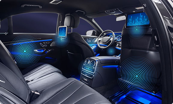
Cabin Experience and Infotainment Solutions
Analog Devices’ innovations for the automotive cabin enable a more immersive, personalized, and safer mobility experience. Our solutions leverage power management ICs, high-performance DSPs, a broad portfolio for automotive connectivity and networking, audio and video converters, sensing, and application-specific software and development tools. This suite of offerings enables large, high-definition displays, advanced audio and acoustic capabilities, driving safety systems, and more.
Explore Applications in Cabin Experience and Infotainment Solutions
-
Rear Seat Entertainment and Cluster Display Solutions

-
Head-Unit and Cockpit ECU Solutions
-
Premium Audio Amplifier Solutions
-
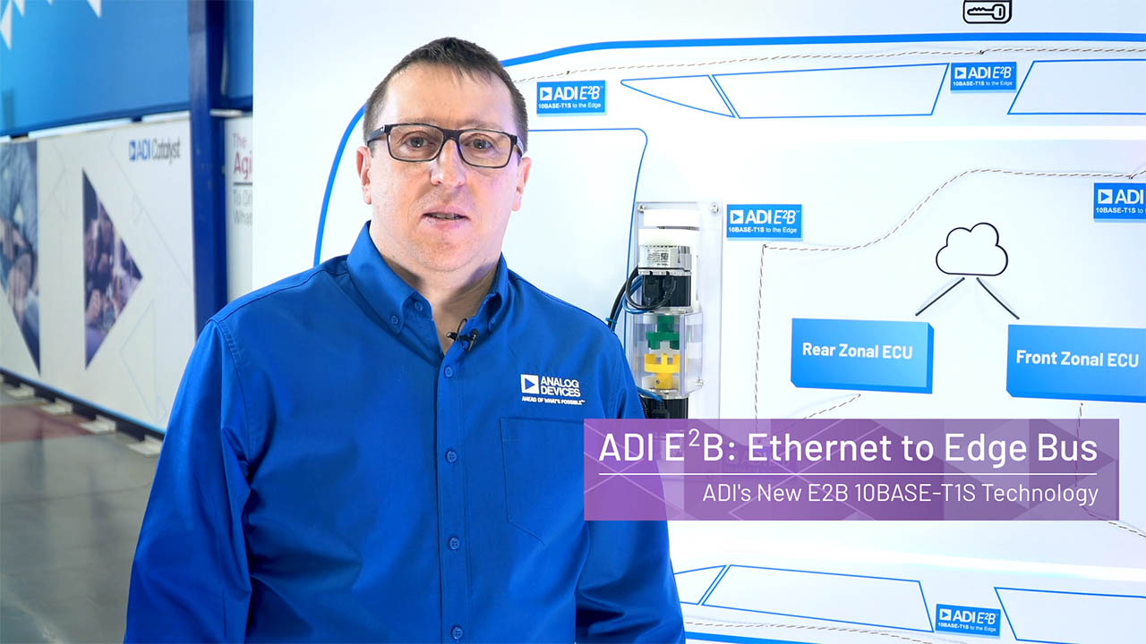
Telematics, eCall, and Networking Solutions
-
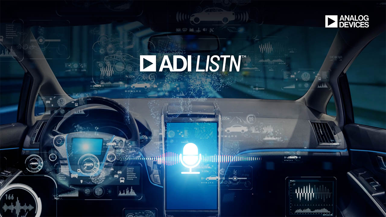
Voice and Acoustic Signal Processing Solutions
-
Automotive Display Solutions


Automotive Power Solutions for Cabin Experience and Infotainment
Designing electronic systems for automotive cabin applications presents many challenges: space is highly restricted, the operating temperature range must be wide, noise must be minimized, battery transients must be tolerated, and quality levels must be high. With integration levels increasing, this creates a need for power-efficient ICs.
Our automotive power management offerings include micropower monolithic buck solutions that provide small form factors, high efficiency, and low noise and EMI to deliver safe operation in high-voltage systems. These ICs help automotive power systems survive harsh load dump and cold crank conditions.
Our product strategy:
- High performance
- High efficiency, low IQ, low EMI
- ASIL solutions for ADAS
- Trusted partner and joint definition
- Scalable high-power density
- Small solution size and BOM optimization
- Lower system BOM cost
Key applications include:
- Car displays and camera connectivity
- Car to cloud communications
- Car audio and acoustics sensing, playback, processing, and distribution
- Car to passenger experience management


Files and Downloads
Application Note

EE-470: ADSP-2156x Power Sequencing Requirements
![]()
2.25 M
EE-444: Guidelines For Optimal Use Of eMSI on ADSP-SC598 SHARC+ Processor Family
![]()
731.39 K
AN-2500: ADA4570 Diagnostic Information
![]()
249.87 K
ZIP
EE-402: Associated Zip File
![]()
202.02 K
EE-402: Synchronous System Halt and Run on the ADSP-CM41x Processor
![]()
580.45 K
Product Highlight
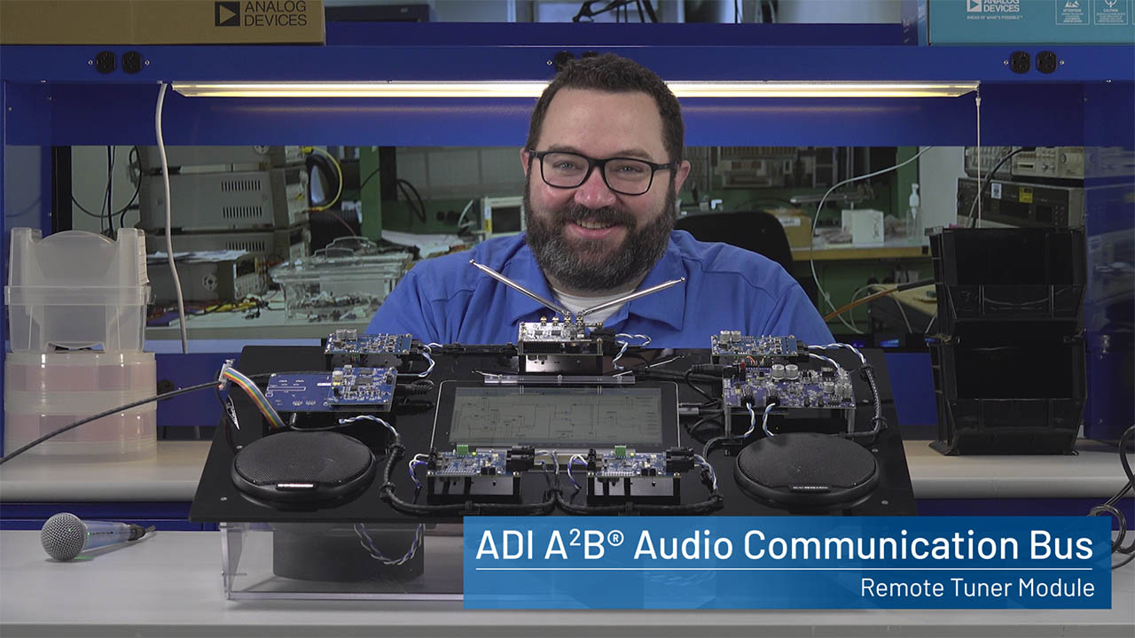
AD2401/AD2402/AD2410 - Automotive Audio Bus Transceivers
![]()
1.43 M
{{modalTitle}}
{{modalDescription}}
{{dropdownTitle}}
- {{defaultSelectedText}} {{#each projectNames}}
- {{name}} {{/each}} {{#if newProjectText}}
-
 {{newProjectText}}
{{/if}}
{{newProjectText}}
{{/if}}
{{newProjectTitle}}
{{projectNameErrorText}}