Versatile New Switching Regulator Fits in SO-8
Introduction
Linear Technology recently introduced the LTC1530 synchronous buck regulator controller. Although packaged in an 8-pin SO, it has proven to be remarkably capable and versatile. The part is loosely based on the popular LTC1430, but with numerous enhancements. Features include current limiting that senses the voltage across the RDS(ON) of the high-side MOSFET (no sense resistor required), built in soft-start, 1% accurate reference, gate drivers capable of handling large MOSFETs, and micropower shutdown. The error amplifier transconductance is higher than that of previous generation parts and is trimmed for accuracy and stabilized over temperature. The IMAX current, which programs current limit, has a positive temperature coefficient to help cancel the positive temperature coefficient of the MOSFET’s RDS(ON). This allows for more consistent current limit over temperature. Although intended primarily for buck regulator designs, the part has been successfully designed into boost, positive-to-negative and negative-to-positive converters.
A Quick Look at the Insides
Figure 1 is the basic block diagram. The LTC1530 is a voltage mode control, synchronous buck regulator controller. An on-chip oscillator generates a 300kHz ramp waveform. The output of the error amplifier is compared to this ramp by the PWM comparator. So far, nothing extraordinary. Current-limit circuitry, however, is a little more unusual. Instead of the traditional current sense resistor, the LTC1530 relies on the RDS(ON) of the high-side MOSFET as its source of load current information. This saves the space, cost and the power dissipation of an additional resistor in the power path. The programming current (IMAX) has a positive temperature coefficient that approximates the positive TC of a MOSFET’s RDS(ON). This tends to flatten the current-limit trip point as a function of temperature. In a slight overload, the LTC1530 provides “square current limiting.” In other words, the regulator starts to look like a current source. In the event of a significant overload, should the output fall to less than one-half of the nominal output voltage, the soft-start capacitor will be discharged very quickly. This forces the regulator into shutdown for a period of time, typically a few milliseconds. After the time delay, the supply attempts to restart. If the overload still exists, the hiccup mode operation will continue. Once the short is removed, the regulator will start normally.
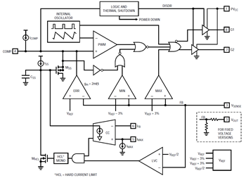
Figure 1. LTC1530 block diagram
Unlike its predecessor, the LTC1530’s soft-start capacitor is internal. The start-up rise time was chosen to satisfy the vast majority of application requirements. Turn on is clean, well controlled and monotonic.
Since dynamic performance is of extreme importance in many of today’s systems, the LTC1530 incorporates several features to provide improved response times to load transients. First are the min/max comparators. These are a pair of comparators that continuously monitor the output voltage. If the output is more than 3% on either side of nominal, the appropriate comparator forces the duty factor to maximum or zero in an attempt to restore the output to the correct level as quickly as possible. Eventually, the error amplifier and main feedback loop will catch up and force the output to settle nicely. The error amplifier is also an improvement over earlier designs. The transconductance and output impedance have both been increased substantially from the LTC1430 values. This has the effect of raising the DC open-loop gain of the amplifier, resulting in better line and load regulation. Transconductance is also trimmed to ensure accuracy. The result is more predictable and repeatable loop response. The amplifier gm is temperature compensated so loop gain stays nearly constant over temperature extremes.
The LTC1530 also has a low power shutdown mode. If the Comp pin is pulled to ground with an open collector or open drain transistor, the LTC1530’s quiescent current will drop to approximately 45µA.
Virtually all integrated circuits have some quirks that will get you in trouble if you don’t pay attention. The LTC1530 is no exception. Care must be taken in choosing the power MOSFETs used in circuits that depend on a charge pump to supply gate-drive power. It is essential to select a FET for the upper device that will be almost fully enhanced before the PVCC supply voltage reaches 8V with whatever main input voltage happens to be available. Failure to heed this requirement can lead to a circuit that may not start up properly at all times. Standard logic-level FETs work fine. Be sure VTH is less than 2V in the worst case.
The cause of this start-up phenomenon is related to the way the current limit circuit behaves. Below a PVCC level of 8V, current limit is disabled. Assume for the sake of this discussion that the main input supply is derived from 5V. At turn on, as the charge pump gradually pushes the PVCC supply upward, the current-limit circuit wakes up at 8V on PVCC. If the 5V supply is exactly 5V, the gate drive available for the FET is only 3V (8V – 5V). If the FET’s RDS(ON) is very high relative to its nominal value at this point, the current-limit circuit may activate in a misguided attempt to maintain control of the output current. If, at the same time, the output voltage has come up to less than one-half of its final value, the LTC1530 will respond by discharging the soft-start capacitor and trying to initiate a restart.
As long as the output voltage has reached a level of greater than one-half of its final value before the PVCC voltage reaches 8V, the output will continue to rise in current limit. If the output is below this level, start-up is not ensured. If the PVCC supply is derived from a 12V source instead of charge pumped from the 5V supply, this problem cannot occur.
A Few Circuit Examples
The LTC1530 turns out to be a rather versatile device. Although intended as a buck regulator, the part has been successfully used in boost and buck-boost designs. Figure 2 is a classic buck topology. The circuit was designed to handle approximately 6A while maintaining a low profile. Input and output capacitors are tantalum devices. The inductor is a very low DC resistance design for high efficiency. The input is 5V, while the output voltage can be jumper selected for 3.3V, 2.5V, 1.8V or 1.5V. The photo in Figure 3 shows the output voltage rise at turn on. A clean, monotonic rise is evident.
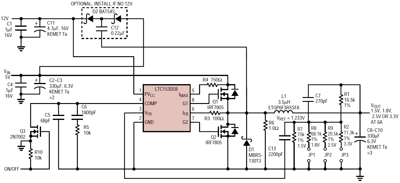
Figure 2. 6A buck regulator; output voltage is jumper selectable for 1.5V, 1.8V, 2.5V or 3.3V
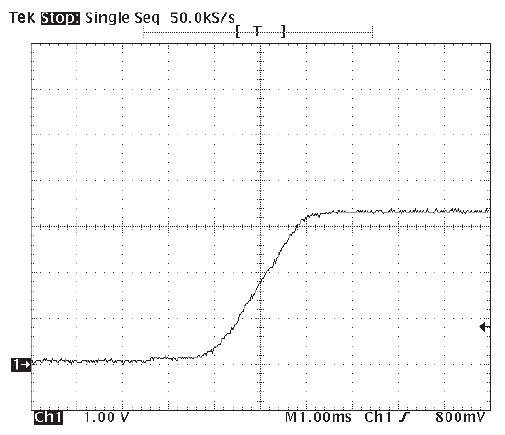
Figure 3. Output voltage at turn-on for Figure 2’s circuit
Figure 4 is a 3A design that has a total height of less than 2.4mm. The inductor is a Gowanda part #50-324, which mounts through a hole in the PCB for a total height above the board of approximately 1.5mm. Output ripple voltage is approximately 10mVP-P at a 3A load with the specified Panasonic SP series output capacitors. There are several options for the main inductor. The overall smallest size available is an IHLP-2525 by Dale Electronics. It’s 3mm tall but only 6.4mm on a side. Output ripple is about 50% higher with this inductor.
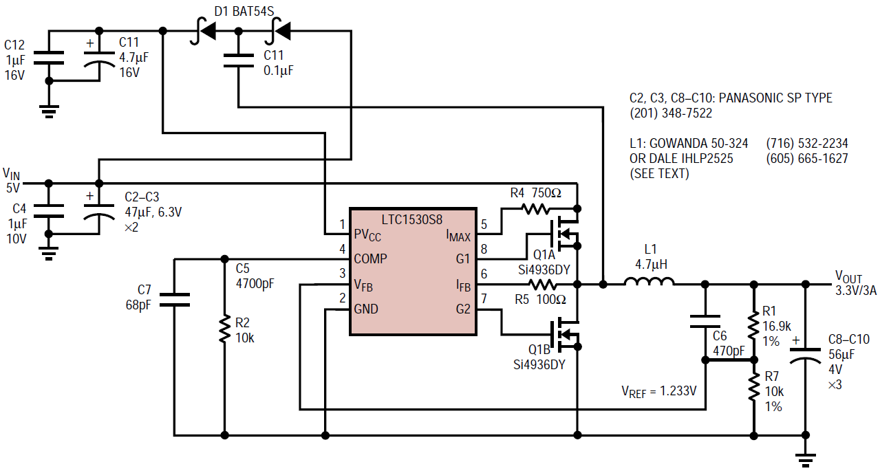
Figure 4. 3.3V/3A regulator
Figure 5 is an example of a synchronous boost regulator. The input is 3.3V and the output is 5V. The circuit is rated for a maximum output current of 6A. Since the output current waveform is discontinuous, the output ripple is inherently large in any boost regulator. The second stage LC filter is added to clean things up a bit. The feedback divider connects to the output before the LC filter for a reason. If the divider is connected after the LC filter, the extra 180° of phase shift above the LC corner frequency will make the regulator’s feedback loop unstable. The DC resistance of the inductor is small, so the effect on load regulation is minimal.
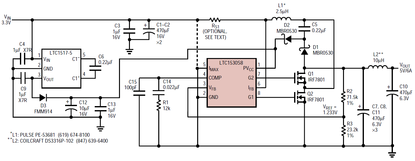
Figure 5. 5V/6A synchronous boost regulator
The LTC1517 charge pump is used to generate a sufficiently high voltage for the LTC1530 to function correctly and also to ensure adequate gate drive for the power MOSFETs. It runs from the 3.3V input and delivers a regulated 5V output. Once the main output comes into regulation, charge pump power is derived through D2. This causes the LTC1517’s regulated output voltage set-point to be exceeded and D3 back biases, shutting the LTC1517 down. Note that current limit is disabled in this design by grounding IMAX and connecting IFB to VIN. Since in the boost topology there is a direct DC path from input to output, there is no point in using the current limit feature except to protect against inductor saturation. It is also worth mentioning that the FET RDS(ON) cannot be used as the current sense resistor in this application because FET Q2’s drain is not common to VIN. If inductor saturation protection is desirable, it is possible to install a small value current sense resistor between C2 and L1. Install an appropriate value resistor (RS1) between C2 and L1; connect the IMAX pin to the C2 side of RS1 (instead of ground) and connect IFB directly to the input side of L1. Just don’t expect the circuit to limit current in the event of a short circuit.
Figure 6 is a positive input to negative 5V output design. Since the LTC1530 needs to be referenced to the –5V output, the design requires external gate-drive circuitry for both the main and synchronous FETs. The absolute maximum voltage rating of the LTC1530’s gate drive would be exceeded if the high-side gate were driven directly. Q3 and the associated parts at the input to the LTC1693 gate driver provide the required level-shift function. The synchronous FET is driven by the other half of the LTC1693. The driver is only required at this location to match the propagation delay of the high-side drive. Failure to pay attention to these details will result in severely degraded efficiency. Output currents of up to 4A can be obtained from this circuit. Like the boost regulator, the output currents are discontinuous, so ripple on the output is somewhat high. A small, second-stage LC filter can easily remedy this if desired.
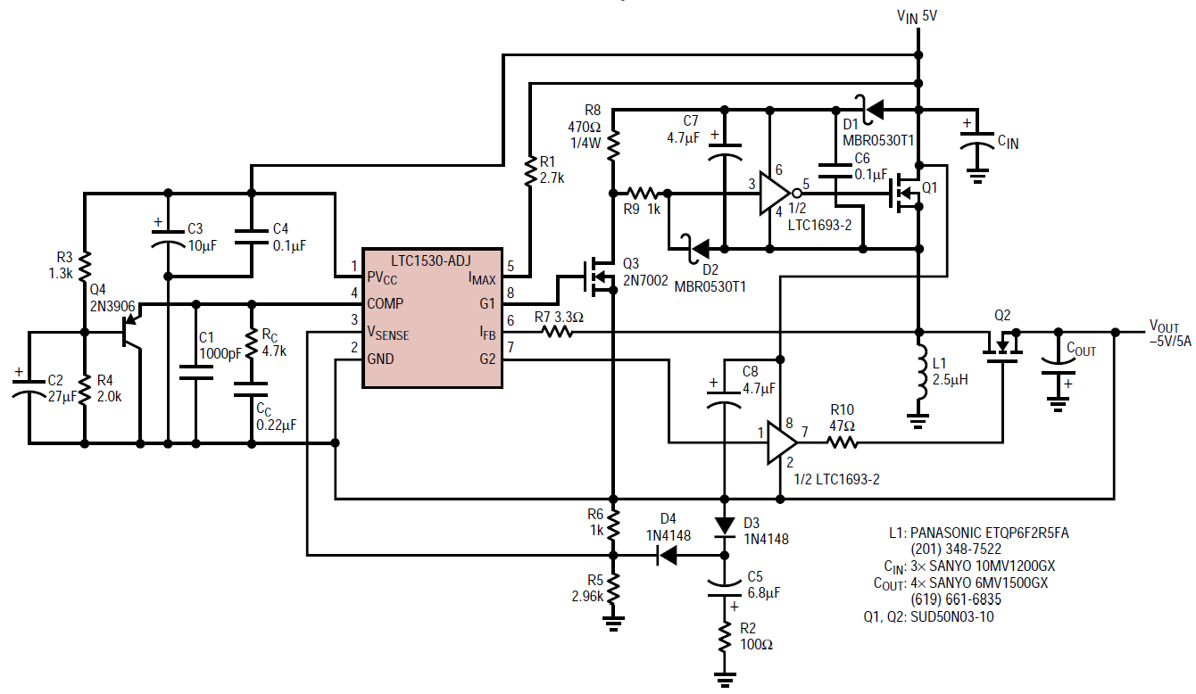
Figure 6. 5V to –5V/4A synchronous switching, inverting polarity converter
Conclusion
The LTC1530 is a small, versatile controller that is usable in numerous topologies and over a wide range of power levels. In the basic buck applications for which it was designed, the LTC1530 permits the designer to realize very simple, low parts count designs that require minimal real estate. The part provides clean turn-on and current-limit characteristics. With a little ingenuity, it is possible to develop circuits different than those that the part’s designers intended, but which give excellent performance nonetheless.


