No-Opto Flyback DC/DC Converters & Snubber Protection Circuits
Flyback Solutions
The flyback DC/DC converter topology is one of several topologies that allow the input voltage to be above or below the output voltage. The SEPIC and buck-boost topologies also allow this, but there are times when a flyback is the more desirable solution: namely when isolation is required (for noise immunity or safety) or when high output voltages are desired. A transformer based flyback is ideal for both; it provides galvanic isolation—there is no direct current path between the input and output, and with the appropriate turns ratio and external components, extremely high voltages can be obtained.
Optocoupler-Based Isolated Flyback Solutions
The circuit below is a typical optocoupler-based isolated flyback solution.
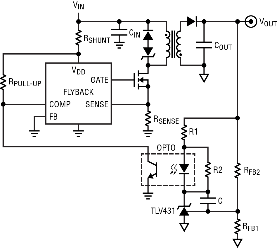
Figure 1. Isolated Flyback Controller with Optocoupler and TLV431 Shunt Regulator
In figure, a controller is used to facilitate high voltage operation. This increases complexity over a monolithic solution, but allows the user to select an external power MOSFET that is appropriate for the desired voltage and allows a low voltage IC to be used since the IC will not be exposed to the high circuit voltages. The output voltage feedback information determined by RFB1 and RFB2 is transmitted across the isolation barrier by way of the optocoupler that is biased with a secondary side TLV431 shunt regulator and resistor R1. A more efficient circuit includes a third winding on the transformer (figure 2) that generates a bias voltage on the primary side to power the IC once the device has started up; this however further increases component count, solution size and cost.
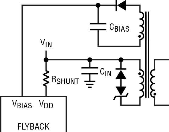
Figure 2. Isolated Flyback Third Winding Circuitry
Many customers are looking for an easy-to-design, small solution size isolated power supply that doesn't require an optocoupler. In addition to increased size and cost, optocouplers dissipate power, have limited dynamic response, and have a current-transfer-ratio (CTR) that degrades over time. More and more engineers are supplanting optocoupler-based solutions with Analog Devices' No-Opto isolated solutions that do not use an optocoupler, yet still provide good output regulation. These solutions have an integrated high voltage power switch, use fewer external components, provide a much smaller solution footprint and have low standby current and higher efficiency than previous solutions.
No-Opto Flyback Solutions
Analog Devices' first generation of No-Opto Flyback controllers greatly simplify isolation circuit design. The optocoupler, shunt regulator and biasing circuitry are no longer needed for isolation, since output voltage feedback information is presented to the IC via the third winding primary of the transformer. However, the still require an external power switch and external an control loop compensation RC network for loop stability.
Analog Devices' latest generation of no-opto, isolated flyback converters expand on the concepts of simplicity, micropower operation and small solution size. The devices feature and internal power switch and range in input voltage from 42V to 560V (42V, 100V and 560V inputs), with 2W to 24W of isolated output power. They use a unique boundary mode control scheme that provides excellent load regulation and control loop stability, reducing the loop compensation circuitry required and minimizing the size of the transformer. As an example, the typical operating circuit for the 100V input, 24W LT8304 is shown below. The LT8304's design simplicity results not only from its control scheme, but also because it has internal control loop compensation and an internal power switch.
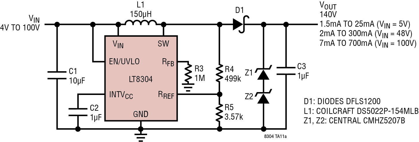
Figure 3. LT8304 Typical Operating Circuit
The output is regulated by monitoring the output voltage reflected back to the inductor's primary side, eliminating the need for an optocoupler and in most cases a third transformer winding (the exception being the 560V input LT8315 which does require a third winding due to its extremely high input voltage range). The result is a relatively high efficiency, tiny, easy-to-design solution with few external components and a small footprint.
The graph below shows the efficiency of the 24W output LT8304 as a function of load current. Efficiencies above 80% are commonplace for this family of devices.
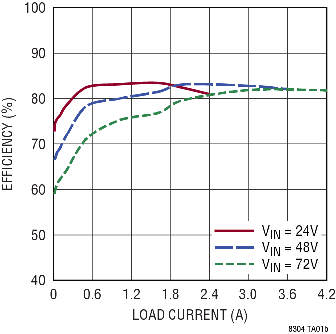
Figure 4. LT8304 Efficiency vs. Load Current
Snubber Circuits
With transformers, primary and secondary side leakage currents can cause excessive voltage spikes that can exceed the absolute maximum voltage rating of the IC and can erroneously trip the power switch control circuitry if allowed to ring for too long. Some inductors have characteristically high leakage inductance, but poorly wound inductors can also exhibit high leakage inductance and the resultant voltage spikes are exacerbated by stray inductance, which is often the result of poor circuit layout. To protect against this, a snubber circuit is used.;
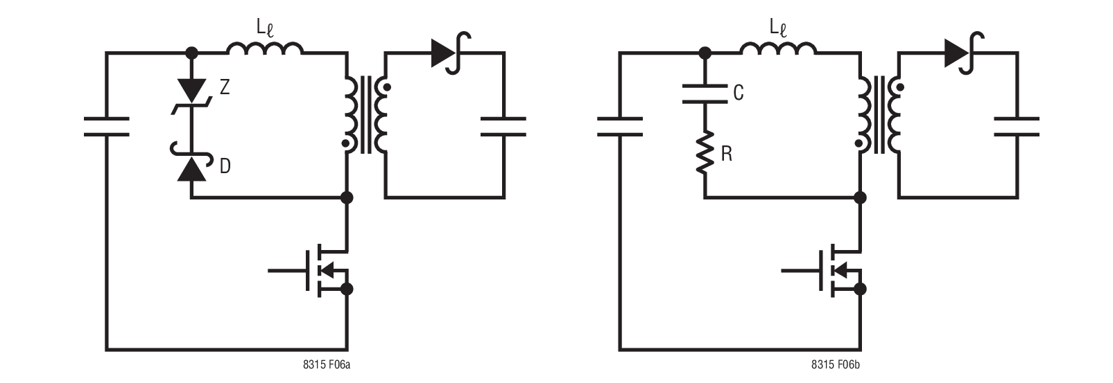
Figure 5. Snubber Circuits
Figure 5 shows two different snubber circuits: a diode-Zener (DZ) snubber and a resistor-capacitor (RC) snubber. A snubber circuit works by absorbing excess energy due to the leakage inductance Ll, thereby protecting the IC from potentially dangerous high voltages or excessive ringing. The DZ snubber ensures a well-defined and consistent clamping voltage and has slightly higher power efficiency, while the RC snubber quickly damps the voltage spike ringing.

Figure 6. Snubber Circuit Waveforms
Figure 6 shows how a snubber circuit provides protection for the LT8304's switch node pin. When designing an application, adequate margin should be kept for the worst-case leakage voltage spikes even under overload conditions. In most cases, the reflected output voltage on the LT8304's primary plus the input voltage should be kept below 110V. This leaves at least 40V margin for the leakage spike across line and load conditions. In figure 6a on the left, no snubber is used, so any ringing must not exceed the upper 150V IC limit. Without any protective circuitry, the performance is left to chance and the possibility of an overvoltage with high input voltages is high since component selection and layout are important considerations. For low input voltage applications, a snubber may not be needed. In figure 6b, a DZ snubber is used. The DZ snubber clamps the switch node pin to 110V using a Zener diode clamp (or a series string of Zener diodes). Note the first amplitude peak (designated by the arrow) has a flattened response due to the Zener clamp. Also note the DZ snubber does not affect ringing, it simply limits the peak voltage. Finally, figure 6c on the right shows the response with an RC snubber. The RC snubber dampens ringing, ensuring oscillations will not inadvertently turn the power switch back on. The LT8304 has a minimum switch on time of 350ns so the ringing must not exceed this minimum limit.
It is common to see either the Zener diode clamp or the RC snubber used in a flyback circuit; and it also is common to see both, as shown in figure 1 above. A snubber circuit is generally recommended when using the high voltage LT8304 to protect the switch node; however, there are special cases when a snubber circuit is not needed, resulting in an even more simplified schematic and a smaller solution footprint. The LT8300 features a 150V/260mA internal power switch and is recommended when small size and fewest external components are key design parameters. It has robust switch protection and includes many circuits in the datasheet that do not include a snubber circuit as shown below in figure 8. . , thus providing the smallest, simplest, lowest power solution for your isolated needs (Figure 7). Here, the switch pin (SW) will see a maximum voltage of VOUT times the turns ratio (8:1) plus VIN, or 3.3V * 8 + 72V, or 96V. This is well below the switch's 150V absolute maximum rating.
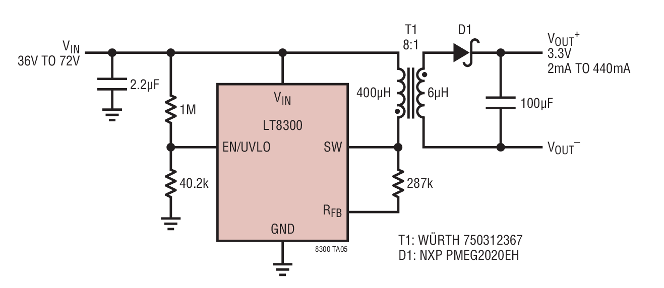
Figure 7. The LT8300 Typically Does Not Require a Snubber Circuit
Conclusion
With the LT83xx family of monolithic, isolated flyback converters, designing a small, efficient, robust, isolated power supply is a fairly simple task. The internal power switch, recommended off-the-shelf transformer and just a few external components all contribute to make the design process easy. A wide range of input voltage and output power combinations are available, which cover output power levels up to 24W. In addition, LTspice files are readily available for circuit simulation, and demonstration circuits provide a convenient way to quickly exercise the solution.
| Part Number | Internal Power Switch | Input Voltage Range (V) | Max Output Power (W) |
| LT8301 | 65V/1.2A | 2.8 to 42 | 6 |
| LT8302 | 65V/3.6A | 2.8 to 42 | 18 |
| LT8304 | 150V/2A | 3 to 100 | 24 |
| LT8300 | 150V/260mA | 6 to 100 | 2.5 |
| LT8303 | 150V/450mA | 5.5 to 100 | 5 |
| LT8315 | 630V/300mA | 18 to 560 | 15 |
