Layout for Power Designs #1: Hot Loops
With two decades field experience supporting mainly industrial and automotive customers, I have a wealth of experience in troubleshooting power supply designs. On customer support you mostly get a call when something does not work as expected or promised in the data sheet. Usually by the time you get the call the layout is already done, lots of money invested and the time to fix things is as tight as the nerves of the project management.
Very often the problems are induced by the layout. On the demo board everything looked and measured fine. But on the customer board where more compromises were made, it's a different story. You could not blame the layout person, who had finished his job by connecting all nodes the schematic called for and got all the components neatly arranged on the PC board. To create a successful power supply layout, some understanding of the physics involved is necessary if you plan to change anything from a proven layout. A demo board layout might be optimized for different requirements than your design, or your design might require slightly different components.
In taking on this blog, I asked myself how to tackle such a broad scoping theme. I think the best approach is to break it into pieces. My goal is to create some intuition what goes on inside your design from the PC-board and component side. During layout phase you often make decisions in seconds which will determine the functionality and EMI of your board. Those decisions can most times not be corrected, even if you desperate use scalpels, rotary cutting tools, copper foil and solder.
I remember about a dozen years ago as a customer was using a switch mode power supply in a car radio for the first time. Many of his colleagues said that it could not be done. However, after a few things were ironed out in layout and input filtering, everything worked fine. Later a customer successfully used an LT1940 1MHz dual step-down switching regulator, which operated in the middle of his AM band in a car radio receiver. No additional metal shielding was required for the power supply unit (PSU), it was only an issue of placement, layout and filtering.
The most important source of EMI in switch mode regulators is the loop where the current is switched. I call it the hot loop.
With non isolated topologies, one of the most basic topologies is the buck regulator. EMI starts off from high di/dt loops. The supply wire as well as the load wire should not have high AC current content. So we can focus our analysis from the input capacitor Cin, which should source all relevant AC currents to the output capacitor Cout, where any AC currents end.
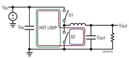
During the on cycle with S1 closed and S2 open, the AC current follows the red loop [Figure 1]. During the off cycle, with S1 open and S2 closed, the AC current follows the blue loop. Both currents have a trapeze shape. People often have difficulty grasping that the loop producing the highest EMI is not the red nor the blue loop. Only in the green loop flows a fully switched AC current, switched from zero to Ipeak and back to zero. We refer to the green loop as a hot loop, since it has the highest AC and EMI energy.
In order to reduce EMI and improve functionality, you need to reduce the radiating effect of the green loop as much as possible. If we could reduce the PC-board area of the green loop to zero and buy an ideal input capacitor with zero impedance, the problem would be solved. But we are limited to the real world. The task of engineering is to find the optimal compromise. The magnetic dipole field strength of this loop is proportional to the current switched and the area covered.
Let’s take a look at the layout of an LT8611 buck converter. The LT8611 has both switches internal, so we only have to be concerned with the connection of the input capacitor.
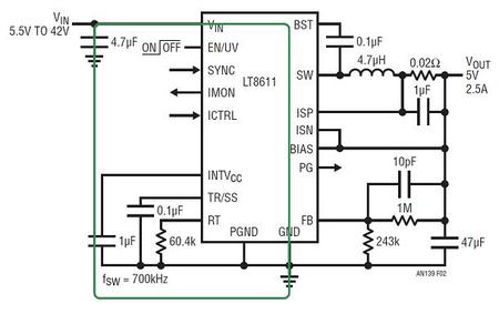
As you can see from the schematic in Figure 2, the hot loop is not easy to spot for layout purposes.
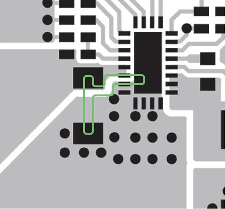
The green line is the hot loop in the top layer. AC currents flows through the input capacitor and the switches in the part. Figure 3 shows the DC1750A LT8611 demo board.
The boost circuit can be viewed in continuous mode as a buck circuit operating backwards.
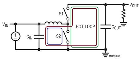
The hot loop is identified as the difference between the blue loop if S2 is closed and the red loop [Figure 4] with S2 open and S1 closed.
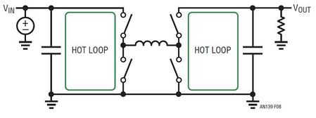
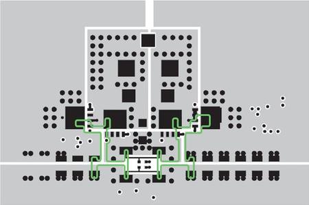
The single inductor 4-switch buck-boost [Figure 5] consists of a buck circuit followed by a boost circuit. The layout will often be complicated by a common GND current shunt which belongs to both hot loops. The LTC3780 DC1046A demo board [Figure 6] shows an elegant solution splitting the sense resistor in two parallel ones.
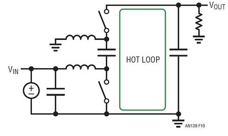
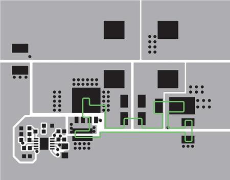
A bit different drawing of a SEPIC circuit [Figure 7] shows its hot loop. Instead of an active MOSFET for the top switch, a diode is often used. The LT3757 DC1341A [Figure 8] shows a good SEPIC layout. The green hot loop area is minimized and has a solid GND plane on the next layer
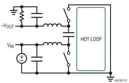
The inverting topology [Figure 9] is very similar to SEPIC [Figure 8], only the load has moved through the top switch and top inductor. Layout is very similar, and demo boards can typically be modified from SEPIC to inverting provided the IC can also regulate on negative feedback voltage like LT3581, LT3757 etc..
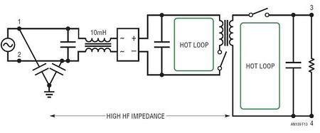
The flyback topology [Figure 10] uses separate windings on a transformer and there is only magnetic coupling between the primary and secondary windings. The current in the primary winding goes to zero with relative high di/dt. Only the energy stored in the leakage inductance and capacitance between windings and on the switch node slows that down. The primary and other transformer windings can be seen as fully switched current. We get two main hot loops as in the buck-boost case [Figure 5]. To reduce EMI, in addition to close VIN decoupling for differential mode EMI, common mode chokes are used for the likely dominant common mode EMI in this topology.
So the first step to a successful layout is to keep the hot loops as small as possible. Use the smallest copper spacing your design rules allow. Use the shortest and flattest ceramic decoupling capacitor which first closes to the hot loop. There is nothing wrong with using several blocking or decoupling capacitors for the hot loop in parallel. You stack them that the shortest and flattest capacitor is close to the hot loop with the larger packages right behind it.


