概览
设计资源
设计与集成文件
- Schematic
- Bill of Materials
- Gerber Files
- Assembly Files
- Allegro Layout File
评估硬件
产品型号带"Z"表示符合RoHS标准。评估此电路需要下列选中的电路板
- EVAL-CN0575-RPIZ ($103.50) 10BASE-T1L Field Instrument Development Board
器件驱动器
软件(如C代码和/或FPGA代码等)用于与元件的数字接口通信。
ADT75 Github Linux Driver Source Code
优势和特点
- Data and Power Delivery using Single Pair Power over Ethernet
- Power Class 12 and 13 Delivery Capable
- Supports Longer Distances up to 1 km
- Provides Speeds up to 10 MBPS
- Works with Existing Software Stacks like PROFINET, EtherCat, MOD-BUS, and others
参考资料
-
EVAL-CN0575-RPIZ User Guide (GitHub)2026/4/16
-
Solutions For Rapid Prototyping: Answering the Needs of Practicing Engineers2023/8/23PDF784 K
电路功能与优势
10BASE-T1L is an Ethernet physical layer standard (IEEE 802.3cg-2019) that is dramatically changing the process and factory automation industry by providing seamless Ethernet connectivity to f ield-level devices including machines, controls, indicators, sensors, and actuators. 10BASE-T1L improves on existing standards such as 4 mA to 20 mA, HART, and FieldBus. Similar to conventional process automation networks, 10BASE-T1L allows both data and DC power to be transmitted over a single twisted pair via single-pair power over Ethernet (SPoE) or Ethernet advanced physical layer (APL).
Compared to traditional methods, 10BASE-T1L offers higher power delivery, higher bandwidth, longer transmission distances, lowercost cabling in new installations, and reuse of 4 mA to 20 mA and RS485 wiring when retrofitting legacy installations. Ethernet supports PROFINET®, EtherCAT/IP, HART/IP, OPC UA™, Modbus®/TCP, and IoT protocols such as message queuing telemetry transport (MQTT). Ethernet also enables simple, centrally controlled software updates right down to the end nodes, which enables faster network commissioning and maintenance.
The circuit shown in Figure 1 is a 10BASE-T1L MAC/PHY interface with SPoE for development of field devices and applications on a Raspberry Pi platform board. The SPoE powered device (PD) and isolated flyback regulator provide 5 V power to the platform board and attached application circuitry. SPoE Class 12 (8.4 W, 24 V nominal) and Class 13 (7.7 W, 55 V nominal) are supported.
The MAC/PHY interfaces to the platform board via serial peripheral interface (SPI), allowing it to be used with microcontrollers and processors that lack an integrated media access control (MAC) layer. The circuit includes a digital temperature sensor, LEDs, and push button, which implement a basic field device example application. The example field device’s drivers are in the Linux industrial input/output (IIO) subsystem, providing a host of debug and development utilities, and cross-platform application programming interface (API) with Python, C, C#, and MATLAB® support.


电路描述
Field Devices
10BASE-T1L is one of the physical layer device (PHY) specifications used in single pair Ethernet that provides a 10 Mbps Ethernet connection over a single twisted pair, up to a length of 1 km. It was defined and developed to be a migration path for the many open and proprietary Fieldbus variants used in process automation such as HART, IO-Link, and Modbus. This allows field instruments and remote I/O devices (for example, sensors, actuators, cameras, machines) to seamlessly communicate with high level control systems via Ethernet. 10BASE-T1L also supports power delivery via SPoE for high power applications, with power levels from 1.23 W at 24 V to 52 W at 54 V.
The CN0575 is a platform for developing Ethernet-capable field devices and applications. Raspberry Pi and Linux provide a rich prototyping and development environment with support for precision data converters, temperature, pressure, flow, acceleration, angular rate sensors, actuators, displays, and I/O devices. This allows a wide variety of field devices to be prototyped and later migrated to a more optimal controller and power solution for the particular application.
Medium Dependent Interface
The single pair Ethernet (SPE) cable, power coupling, filtering, and data coupling network to the MAC-PHY forms the medium dependent interface (MDI) of the CN0575. For 10BASE-T1L systems that support SPoE, this circuit is usually comprised of a mechanical connector, common-mode and differential-mode interface chokes, coupling capacitors, and data isolation transformers. Figure 2 shows a simplified diagram of the MDI used in the CN0575. Proper selection of the MDI components is critical to minimize losses and to preserve the integrity of the data signals.

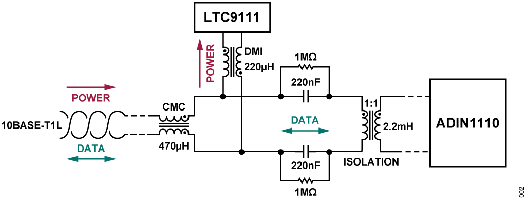
The common-mode choke (CMC) in the MDI suppresses commonmode noise that may be coupled into the SPE cable from the environment, while passing the differential data and power. As such, it is important to select a device that has a high common-mode impedance and a low differential-mode impedance in the 10BASE-T1L frequency range (0.1 MHz to 20 MHz). Since the common-mode choke is placed in series with the SPE cable, the device must be rated to handle the maximum cable current specified for the PD class being used (that is, 632 mA for Class 12; and 231 mA for Class 13).
The core capability of the 10BASE-T1L is a full duplex, DC balanced, point-to-point communication scheme with pulse-amplitude modulation 3 (PAM-3) at a 7.5 MBd symbol rate with 4B3T coding. It supports two amplitude modes: 2.4 V peak-to-peak for a cable up to 1000 meters and 1.0 V peak-to-peak at a reduced distance. Power and data are separated via inductive (DC) coupling and transformer (AC) coupling, respectively. SPoE power is extracted by a differential mode coupled inductor (DMI). Similar to the common- mode choke, it must also have a maximum current rating appropriate for the PD class in use, and low DC resistance to minimize power loss. Data is coupled to the PHY by an isolation transformer.
The isolation transformer's inductance is in parallel with the DMI's inductance; the total inductance must be high enough to avoid significant loading at frequencies of 7.5 MHz and higher. The IEEE 802.3dd-2022 amendment specifies a maximum signal droop of 25%. The DMI inductance in the CN0575 is 220 μH and the isolation transformer's inductance is 2200 μH, or 200 μH total. This results in a maximum droop of 10%, maintaining signal integrity and easily meeting the 25% specification.
10BASE-T1L MAC-PHY Circuit
The ADIN1110 provides the 10 Mbps, full-duplex, single-pair Ethernet connectivity in the CN0575. As shown in Figure 3, this device combines a 10BASE-T1L PHY and its associated subsystems with an Ethernet MAC that can directly communicate with the host processor via SPI. This allows the ADIN1110 to be used with low power processors that have no built-in MAC. The SPI bus can operate up to 25 MHz, enabling the full 10 Mbps bandwidth of the 10BASE-T1L interface, with margin.

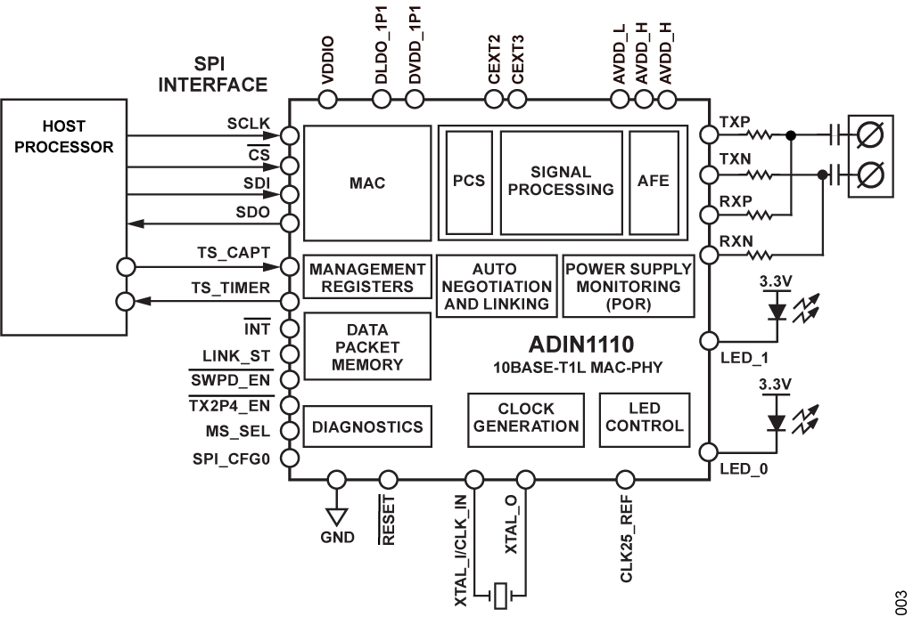
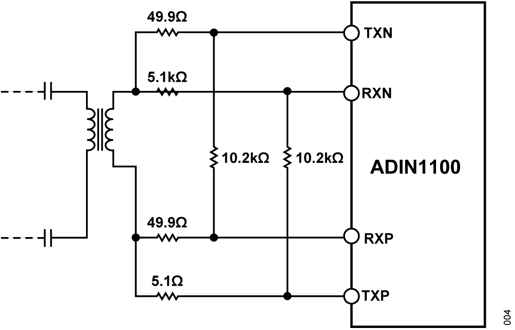
The MDI pins, TXP, TXN, RXP, and RXN, connect the ADIN1110 PHY to the Ethernet network via the 10BASE-T1L cable. For proper operation of the ADIN1110, an external hybrid must be placed between these pins and the cable coupling network. Figure 4 shows the required topology and values specified in the ADIN1110 data sheet for this hybrid.

The ADIN1110 has four supply domains that power the different sections of its internal circuitry, and their connections may vary based on the requirements of the application. AVDD_H and AVDD_L can be set to either 3.3 V or 1.8 V depending on the transmit level mode that needs to be supported, and VDDIO must be set to the SPI voltage level used by the host processor. DVDS_1P1 should normally be shorted to the output of the internal low dropout (LDO) regulator, but can be connected to an external supply instead for better power efficiency in systems with multiple ADIN1110 devices.
In CN0575, AVDD_H, AVDD_L and VDDIO are all tied to 3.3 V, while DVDD_1P1 is connected to the output of the internal LDO regulator. This configuration eliminates the need to include additional LDO regulators, while at the same time allowing the ADIN1110 PHY to support both 2.4 VP-P and 1.0 VP-P transmit level modes in the 10BASE-T1L link.
The ADIN1110 requires a 25 MHz reference signal to generate the different internal clocks needed for its operation. In CN0575, this signal is produced by a 25 MHz crystal with a tolerance rating of ±10 ppm, a stability rating of ±20 ppm, a maximum ESR of 50 Ω, a maximum drive level of 100 μW, and a load capacitance rating of 10 pF well within the requirements of the ADIN1110. Refer to the ADIN1110 data sheet for details.
Configuring the 10BASE-T1L MAC-PHY
An autonegotiation process is defined in the IEEE 802.3-2022 standard to bring up and link with another 10BASE-T1L device. This handshaking mechanism enables the ADIN1110 and its link partner to advertise their Ethernet capabilities, compare them, and then identify the best operating mode that both devices can support. For a 10BASE-T1L link, one of the parameters that both PHYs need to agree on is the transmit level. Typically, a 10BASE-T1L link uses the standard 1.0 VP-P level; the higher 2.4 VP-P level can only be used if at least one PHY requests for it and both devices advertise capability of supporting its operation. By default, the CN0575 advertises support for both transmit levels. Autonegotiation also allows the ADIN1110 PHY and its link partner to establish their controller/peripheral relationship. During this process, the two PHYs advertise their preferred modes and compare them. If their preferences are different, the PHYs are configured accordingly. Otherwise, the controller and peripheral assignments will be randomly assigned.
For the ADIN1110, the default advertised controller/peripheral preference during autonegotiation is determined by the logic level of the TS_TIMER/MS_SEL pin, which is normally held at logic low by an internal pull-down resistor.
For most applications, the actual controller/peripheral configuration of the two devices is unimportant. Similar to how a 2.4 VP-P transmit level operation is requested, the ADIN1110 PHY can be forced to use its preferred controller/peripheral by setting the appropriate bit in the 10BASE-T1L autonegotiation advertisement register, if needed. In this case, the link partner is configured into the opposite mode during the autonegotiation process. It should be noted that if the link partner is set up such that it is forced to use the same controller/peripheral configuration, then a fault occurs, and the autonegotiation process fails.
The ADIN1110 PHY can be reconfigured to advertise a different transmit level capability and controller/peripheral configuration preference if the default settings do not meet the application requirements. To do this, the following procedure should be done prior to bringing up a link:
- Place the ADIN1110 into software power-down mode using the software power-down control register.
- Access the PHY registers via the MDIO access registers to produce the desired configuration.
- Exit software power-down mode to initiate autonegotiation.
The ADIN1110 can also be placed immediately into software power- down mode after a reset operation by pulling the SWPD_EN pin high. For added flexibility, the CN0575 allows the user to select the software power down mode. This provides an easy way to implement or skip software power-down as needed. For more details on the ADIN1110 registers, refer to the device data sheet. Table 1 summarizes how to select the initial operating mode of the ADIN1110 PHY core using the different mode selection pins. The CN0575's default configuration maximizes the compatibility with most controller configurations.
Table 1 summarizes how to select the initial operating mode of the ADIN1110 PHY core using the different mode selection pins. The CN0575's default configuration maximizes the compatibility with most controller configurations.
| ADIN1110 Pin | Logic Level | Operating Mode |
|---|---|---|
| TX2P4_EN | High | Only 1.0 VP-Ptransmit level is supported. |
| Low | Both 1.0 VP-Pand 2.4 VP-P transmit levels are supported. Default for CN0575. | |
| TS_TIMER/ MS_SEL | High | PHY prefers to be configured as a controller device. |
| Low | PHY prefers to be configured as a peripheral device. Default for CN0575. | |
| SWPD_EN | High | PHY immediately starts autonegotiation after reset. |
| Low | PHY enters software power-down mode after reset. Default for CN0575. |
Single-Pair Power Over Ethernet
Single-pair power over Ethernet is an Ethernet network implementation that uses a unique PHY transceiver over a twisted pair of wires. It provides power over the existing data cabling structure and is defined to work with the 10BASE-T1L 10 Mbps protocol.
SPoE is an extension of the power over data line (PoDL) standard originally defined for use in automotive networks. The new standard adds power classes 10 to 15, intended for use in industrial networks that have either 24 V or 55 V nominal DC power available. These power classes that standardize the power sourcing equipment (PSE) output voltage range and the maximum power that can be delivered to a PD, as shown in Table 2.
| Class | 10 | 11 | 12 | 13 | 14 | 15 |
|---|---|---|---|---|---|---|
| VPSE(V, min/typ/max) | 20/24/30 | 50/55/58 | ||||
| ICABLE(mA, max) | 92 | 240 | 632 | 231 | 600 | 1579 |
| PPD(W, max) | 1.23 | 3.2 | 8.4 | 7.7 | 20 | 52 |
| RCABLE(Ω, max) | 65 | 25 | 9.5 | 65 | 25 | 9.5 |
This Ethernet capability builds on traditional power over Ethernet (PoE) and can be easily installed and maintained. The SPoE compliant switches and endpoints ensure network additions and upgrades are simple and fast. Moreover, it reduces system cost, weight, wiring complexity, and power when compared to traditional Ethernet cabling.
SPOE Powered Device Controller
An LTC9111 SPoE PD controller is used to communicate with a PSE via the serial communication classification protocol (SCCP) and negotiate the power allocation for the CN0575. The PD power class advertised by the LTC9111 is determined by the logic levels of its CLASSV and CLASSC pins, which can be configured to three different states (shorted to GND, shorted to STBY voltage, or left floating).
The CN0575 is designed to operate as either a Class 12 or Class 13 PD, with the class selection being implemented using jumpers connected to the configuration pins.
Input Polarity Correction
IEEE 802.3cg requires polarity insensitive PDs to facilitate foolproof field installation with screw terminals. The LTC9111 drives external MOSFETs (M2 and M3 in Figure 5) for polarity correction on the low-side and relies on external Schottky diodes (DIN1 and DIN2) to rectify the high-side voltage. Active low-side rectification minimizes power losses and also helps overcome circuit start-up challenges posed by the constraints of the standard. The drive voltage at the LGATE1 and LGATE2 pins is compatible with modern standard-level power MOSFETs. These MOSFETs do not experience high voltage and high current simultaneously, so safe operating area (SOA) performance is not critical.


External MOSFET Switch and Inrush Control
The external N-channel MOSFET switch (M1) functions as an inrush controller and load switch, isolating the bulk capacitance from the connector during classification and ramp up. Once the operating voltage exceeds the device threshold for the selected power class (17.5 V Typ. for Class 12; 46 V Typ. for Class 13), an internal 10 μA (14 μA maximum) charge pump is enabled after a 100 ms delay. M1 then acts as a source follower, and CBULK voltage linearly increases until M1 is fully enhanced.
Use Equation 1 to ensure that the inrush current does not exceed the maximum PD current for the corresponding class.

where:
- CGATE is the capacitance between RGATE and GND.
- CBULK is the capacitance between OUT and GND.
- IGATEUP(MAX) is the maximum GATE pull-up current of the LTC9111.
- ICLASS(MAX) is the maximum PD current for the selected power class.
During inrush, there can be significant transient power dissipation in the external MOSFET; SOA capability must be considered in selecting the pass device. Any load present at the OUT pin before inrush is complete also contribute to the total PD current observed at the connector; this may necessitate slower inrush (that is, larger CGATE). The MOSFET used for this switch in CN0575 is able to withstand the maximum current drain current of 11.5 A of the selected power class, as well as the transient power dissipation of 60 V, 1 A for at least 100 μs.
A resistor, RGATE, in series with CGATE, is recommended for robustness. As an example, a fault which shorts the OUT pin to ground instantaneously while power is applied will pull the source of the external MOSFET to ground while CGATE maintains high voltage at the GATE pin, causing stress on the gate of the external MOSFET. A resistor value of RGATE = 10 k will effectively decouple the gate of the MOSFET from the capacitor in such a scenario.
The EN logic output is used to ensure that the downstream switching regulator (or other application circuitry) does not draw significant current until inrush is complete. The EN pin is driven high once GATE exceeds IN by 6.5 V, at which point M1 is fully enhanced and full load current can be drawn.
Isolated Flyback Converter Circuit Design
An LT8304 flyback converter is used to supply the 5 V power required by the host Raspberry Pi. This device can accept an input voltage between 3 V and 100 V and deliver up to 24 W of isolated output power, allowing it to easily operate in SPoE PD Classes 12 and 13. Figure 6 shows the isolated flyback circuit configuration for the CN0575.


In CN0575, the LT8304 uses a flyback transformer with a turns ratio of 6:1 and a primary inductance of 40 μH to produce the isolated power. As recommended in the LT8304 data sheet, an RC and Schottky/Zener snubber is additionally connected across the primary windings of the transformer to protect the device from high voltage spikes generated by leakage inductance. A diode is used to provide rectification on the secondary side, and is rated for a forward current of 10 A and a reverse voltage of 45 V. Three 100 μF capacitors are used to reduce the ripple of the output voltage. This combination of components allows the design to meet the power requirements for Class 12 and Class 13 devices, as well as support the operating requirements of the LT8304. For the general design procedure in selecting these components, refer to the LT8304 data sheet.
The output voltage of the LT8304 is set by an external feedback resistor connected between the SW and RFB pins; the value of which is calculated using Equation 2:

where:
- RFB is the feedbafigck resistance in kΩ.
- RREF is the reference resistance in kΩ.
- VREF is the internal reference voltage in V.
- NPS is the transformer effective primary-to-secondary turns ratio.
- VOUT is the output voltage.
- VF is the output diode forward voltage.
For the required output voltage of 5 V, a 6:1 transformer turns ratio, 1 V VREF, 10 k RREF, and an output diode forward voltage of 0.3 V, the equation results in an RFB value of 318 kΩ; the closest standard 1% value of 316 kΩ is used.
As shown in Figure 7, these specifications allow the LT8304 to supply more than 2 A of load current — more than adequate for Classes 12 and 13, which only require 1.68 A and 1.54 A, respectively for 5 V.


Minimal Field Device
The CN0575 can be used as a basic temperature sensing field device using an on-board ADT75 digital temperature sensor. This device is ideal for a minimal complete temperature monitoring application. The only external components required for its operation are a decoupling capacitor for the supply pin, and pull-up resistors for the I2C lines.
In addition to the ADT75, the CN0575 also includes a push button and an LED as basic GPIO devices that can be used to provide remote user input/output. Additional Raspberry Pi peripheral hardware devices can be used to prototype other field device applications once basic connectivity has been established.
常见变化
While the CN0575 is intended to operate in either SPoE PD classes other than 12 or 13, the LTC9111 PD controller supports all PD classes from 10 and 15. The isolated power supply can then be optimized for the power level required by the end application.
For applications not requiring galvanic isolation, or where the isolated circuitry is low power, the ADIN1110 PHY can be capacitively coupled to the MDI. In this topology, the isolation barrier can be placed between the microprocessor and sensor, ADC, or DAC using a digital isolator such as the ADuM5411.
For applications such as field switches and building/room controllers where the processor has an integrated MAC, the ADIN1100 can be used instead. This is a 10BASE-T1L PHY device with MII, RMII, and RGMII MAC drivers for development with existing interfaces.
电路评估与测试
This section covers the setup and procedure for evaluating the CN0575 circuit evaluation board using a Raspberry Pi. For complete details, refer to the EVAL-CN0575-RPIZ User Guide.
Equipment Needed
- EVAL-CN0575-RPIZ
- EVAL-ADIN1100-EBZ
- 24 V (Class 12) or 55 V (Class 13) power supply
- Raspberry Pi computer (Model 3B+ or above)
- Host PC (Windows/Linux/Mac)
- CN0575 demo Python script
- Plug-in screw-terminal connector
- Single-pair of 18 AWG (max) wires
- Category 5e Ethernet cable with RJ45 connectors
- USB-A to micro-USB-B cable
Getting Started
Before proceeding with the test, the Raspberry Pi must be configured with the latest ADI Kuiper Linux image and set to use the CN0575 device tree. For a detailed procedure on how to set up the Raspberry Pi, refer to the EVAL-CN0575-RPIZ User Guide.
Setup and Test
To establish a 10BASE-T1L connection to a Raspberry Pi using the EVAL-CN0575-RPIZ, follow below procedure:
- Connect the EVAL-CN0575-RPIZ to the Raspberry Pi via the 40-pin interface connector.
- Set the output of the DC power supply to either 24 V (Class 12) or 55 V (Class 13), depending on the setting of JP1 and JP2 on the EVAL-CN0575-RPIZ.
- Screw in one end of the single pair of wires to the terminal block of the EVAL-CN0575-RPIZ.
- Screw in the other end to the plug-in connector on the EVAL-ADIN1100- EBZ.
- Screw in the other end of the twisted pair into the EVAL-ADIN1100- EBZ 10BASE-T1L terminal block.
- Using the Ethernet cable and the micro-USB cable, connect the EVAL-ADIN1100-EBZ to the host PC

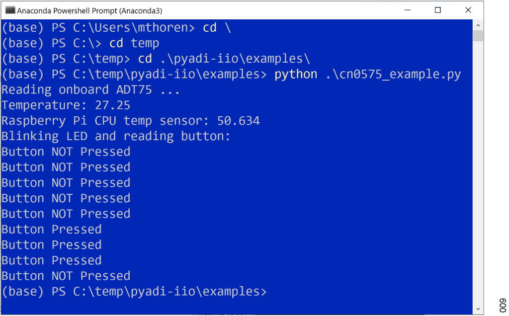
Figure 8. CN0575 Test Setup - The LINK LED on the EVAL-CN0575-RPIZ and the LED_0 LED on the EVAL-ADIN1100-EBZ must turn on and start blinking at the same time to indicate a successful link.
- On the host PC, use remote access software (PuTTY, VNC viewer) to log into and control the Raspberry Pi.
- Open Python on the remote host and run the CN0575 example script, as shown in Figure 9. The CPU temperature and ADT75 will display, the on-board ALERT LED starts blinking, and the state of the TEST button will be displayed.