概览
设计资源
评估硬件
产品型号带"Z"表示符合RoHS标准。评估此电路需要下列选中的电路板
- CFTL-LED-BAR ($67.68) 3-Channel RGB LED Board
- EVAL-ADICUP3029 ($60.92) Arduino Form Factor Development Board
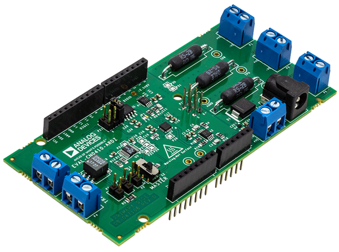
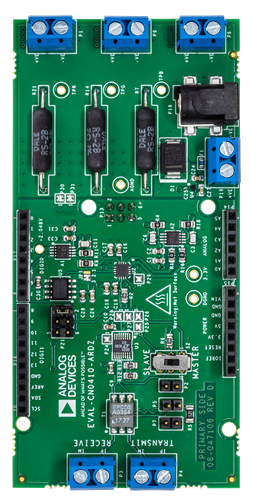
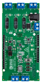
- EVAL-CN0410-ARDZ ($101.52) 3-Channel LED Driver Board
参考资料
-
User Guide: EVAL-CN0410-ARDZ Shield2018/6/28WIKI
-
CN0410: Programmable, 3-Channel LED Current Source Driver with isoSPI Repeater2018/6/21PDF267 K
电路功能与优势
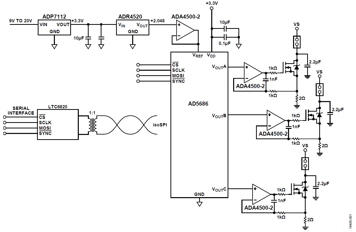
The circuit shown in Figure 1 is a 3-channel, programmable, LED current driver with digital communications repeater cababilites.
Each of the three output channels is controlled by a single digital-to-analog converter (DAC), which simplifies the digital communications and reduces cost. Each channel can be individually programmed and is capable of sourcing 1 A of current through its load.The circuit also has an isoSPI™ repeater that allows multiple boards to be controlled with a single master. The repeater translates the serial port interface (SPI) signals into pulses that are transmitted through a twisted pair of wire and converted back to an SPI signal at the other end.
This solution is ideal for precision lighting control applications where a compact, scalable, single-supply, and highly linear, 3-channel, 16-bit buffered current source is required.
电路描述
Digital-to-Analog Converter Output
Figure 1 shows the single-supply signal chain that consists of a voltage reference, a DAC, a DAC buffer, voltage to current conversion stage, and an isolated SPI communication interface.
The DAC is the AD5686, a low power, quad, 16-bit, buffered voltage output DAC. The output voltage of the DAC is dependent on the reference voltage, as shown in the following equation:

where
D is the decimal data word loaded in the DAC register.
N is the number of bits.
For a reference of 2.048 V, and N = 16, the equation simplifies to the following:

This equation gives a VOUT of 1.024 V at mid scale, and 2.048 V at full scale.
The LSB size is 2.048 V/65,536 = 31.25 μV.
One LSB at 16 bits is also 0.0015% of full scale or 15 ppm of full scale.
The DAC reference pin is driven by a 2.0248 V reference device, the ADR4520B. The ADR4520B voltage reference provides a high precision, low noise (1 μV p-p, 0.1 Hz to 10 Hz) and stable reference to the DAC. The ADR4520B uses an innovative core topology to achieve high accuracy, temperature stability, and noise performance. The low output voltage temperature coefficient (2 ppm/°C maximum) and low long-term output voltage drift of the device also improve system accuracy over time and temperature variations. The initial room temperature accuracy of the ADR4520B is ±0.02% maximum, which is approximately 13 LSBs at 16 bits.
Voltage to Current Conversion
The ADA4500-2 is selected as the operational amplifier. This device is a high precision amplifier with a maximum offset voltage of 120 μV, offset drift of less than 5.5 μV/°C, 0.1 Hz to 10 Hz noise of 2 μV p-p, and maximum input bias current of 2 pA. Its key feature of rail-to-rail input and output swing with zero crossover distortion makes the ADA4500-2 a suitable candidate for this function.
A typical rail-to-rail input amplifier uses two differential pairs to achieve rail-to-rail input swing (see the MT-035 Tutorial). One differential pair is active at the higher range of the input common-mode voltage, and the other pair is active at the lower end. This classic dual differential pair topology introduces crossover distortion during the handoff of one differential pair to the other. The change in offset voltage causes nonlinearity when the amplifier is used as a DAC buffer. The ADA4500-2 uses an integrated charge pump in its input structure to achieve rail-to-rail input swing without the need for a second differential pair. Therefore, it does not exhibit crossover distortion. Using a zero crossover distortion amplifier in this single-supply system provides wide dynamic output range while maintaining linearity over the input common mode/input digital code range. Details of the operation of the ADA4500-2 can be found in the ADA4500-2 data sheet.
The ADA4500-2 is a suitable candidate with high input impedance, 2 pA maximum input bias current at room temperature, and 190 pA maximum input bias current over temperature. This low bias current results in 1.2 μV of worst-case error due to input bias current, which is much less than 1 LSB.
The output the DAC is buffered and used to turn on the MOSFET, with feedback taken from the current sense resistor. A current source must be compensated properly to prevent oscillations when driving an inductive load such as the wiring to the LED board. The Rx resistor, Ry, resistor, Cx capacitor, and Cy output capacitor provide frequency compensation. This circuit tolerates a load inductance of up to 5 μH. (For example, an LED board wired to the CN-0410, located 5 m away, with 16-gauge wire, spaced 10 mm apart, is approximately 5.5 μH. Most practical installations have conductors much closer together, and therefore lower inductance.) An LTspice® simulation is provided to aid in compensating for other loads.
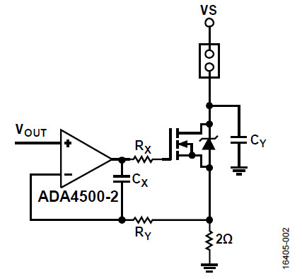
The circuit in Figure 2 converts the control voltage from the DAC into a current that drives the LED. The MOSFET in the circuit is able to handle currents of up to 6.3 A. However, the current is limited to 1 A, which is the maximum rated current of the LED.
The maximum current is limited by the resistors on each channel: R7, R14, and R21. The maximum current can be calculated by

where R = 2 Ω.
Power Dissipation and Thermal Considerations
When driving LEDs with a linear current source, the power dissipation of the sense resistors and MOSFETs must be considered. Power dissipation in the sense resistors is always less than their 3 W rating, even at the maximum setpoint current of 1 A. MOSFET power dissipation increases if the LED supply voltage is increased, resulting in more voltage drop across the MOSFET. When used with the CFTL-LED-BAR and a supply voltage of 16 V, keeping below half scale (500 mA) reduces dissipation. Under these conditions, the board temperature reaches approximately 79°C in the vicinity of the MOSFETS with the board positioned vertically in still air. The LTspice simulation can also be used to estimate power dissipation for other load conditions.
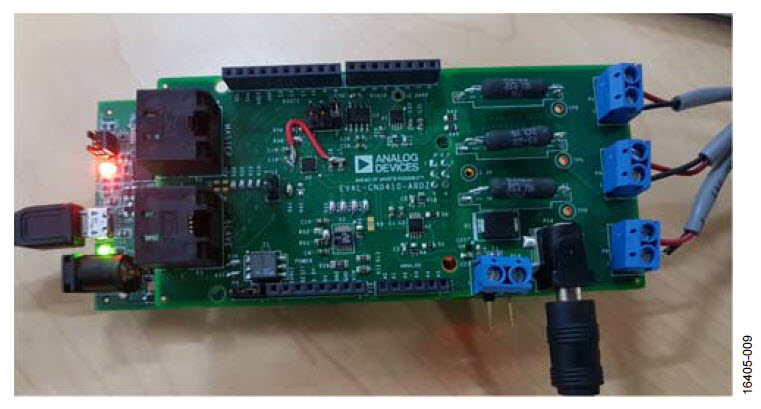
For higher power levels, a heat sink or forced convective cooling (fan) may be required to keep the board temperature lower than 130°C, the recommended maximum for FR-4. Figure 3 shows the board operating in free air, at half of its maximum power on Channel A at 500 mA, with an input voltage of 16 V.
The resistors reach 95°C, and the area around the FETs is approximately 79°C.
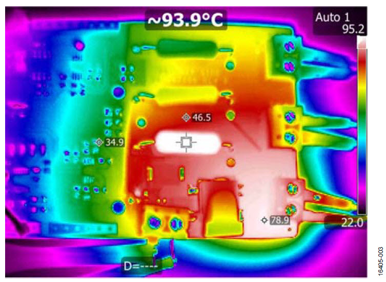
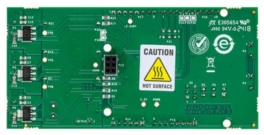
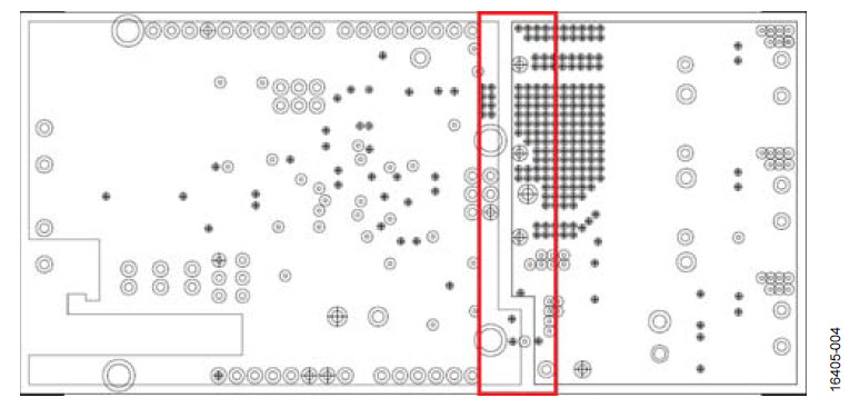
The board has as an area where there is no copper pour (shown in Figure 4), which acts as a thermal isolation barrier from the rest of the circuit. This area can be seen in Figure 3, where there is a drastic drop in temperature across the two ground planes. This barrier helps keep the temperature drift due to the components on the left side of the board to its minimum.
Isolated Daisy-Chained SPI Control
The circuit also has a SPI communications protocol repeater, which is enabled by the LTC6820. This device enables multiple boards to be connected to a single twisted pair cable with only one master controlling the whole chain.
The LTC6820 provides bidirectional SPI communications between two isolated devices through a single twisted pair connection. Each LTC6820 encodes logic states into signals that are transmitted across an isolation barrier to another LTC6820.
The receiving LTC6820 decodes the transmission and drives the slave bus to the appropriate logic states. The isolation barrier is bridged by a simple pulse transformer to achieve basic isolation on the CN-0410. With layout optimization, an isolation voltage of 1500 V can be achieved, limited by the transformer. Refer to the LTC6820 for other recommended transformers.
The LTC6820 drives differential signals using matched source and sink currents, eliminating the requirement for a transformer center tap and reducing electromagnetic interference (EMI). Precision window comparators in the receiver detect the differential signals.
The drive currents and the comparator thresholds are set by a simple external resistor divider, allowing the system to be optimized for required cable lengths and desired signal-to-noise performance.
Integral Nonlinearity (INL) and Differential Nonlinearity (DNL) Measurements
Measured results show that the combination of the AD5686, ADR4520B, and ADA4500-2 is an excellent solution for high accuracy, low noise performance applications. The ADA4500-2 maintains the linearity of the DAC with no crossover distortion.
INL error is the deviation in LSB of the actual DAC transfer function from an idealized transfer function. DNL error is the difference between an actual step size and the ideal value of 1 LSB. This system solution provides a 16-bit resolution with ±1 LSB DNL and INL. Figure 5 and Figure 6 show the DNL and INL performance of the circuit.
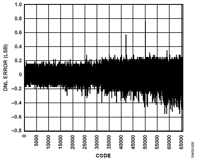
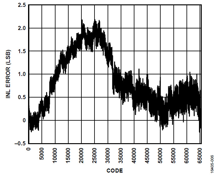
Note that the DNL and INL measurements exclude the 100 codes (approximately 4 mV) from the lower end of the range, because the rail-to-rail output stage becomes nonlinear over this region, as described in MT-035 Tutorial.
Noise Measurements
The targeted 0.1 Hz to 10 Hz noise for the whole board is to be less than 24 μV p-p. The AD5686, ADA4500-2, and ADR4520B contribute a calculated total of 9 μV p-p to the whole circuit. The true noise of the circuit is measured by using a noise measuring box with a gain of 10,000 and filtered between 0.1 Hz and 10 Hz.
It is advised to take the cleanest supply when taking the noise measurements. Therefore, the ADICUP3029 was removed from the setup, and the supply is taken from a 9 V battery.
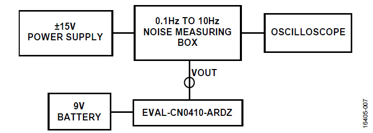
The noise of the box itself and the circuit with the noise box were measured, and their noises are 4.22 μV p-p and 8.38 μV p-p, respectively. Uncorrelated, Gaussian noise sources add in a root sum square (RSS) manner. Therefore, the noise of the CN-0410 is

Using this equation, the true noise of the circuit is calculated to be 7.23 μV p-p.
Board Layout Considerations
It is important to carefully consider the power supply and ground return layout on the board. It is recommended that the printed circuit board (PCB) have separate analog and digital sections. If the circuit is used in a system where multiple devices require an analog ground to digital ground connection, make the connection at only one point. Bypass all power supply pins with at least 0.1 μF capacitors. Place these bypass capacitors as physically close as possible to the device, with the capacitor ideally right up against the device. Choose the 0.1 μF capacitor to have low effective series resistance (ESR) and low effective series inductance (ESL), such as ceramic capacitors. This 0.1 μF capacitor provides a low impedance path to ground for transient currents. Use large traces for the power supply lines to provide a low impedance supply path. Use proper layout, grounding, and decoupling techniques to achieve optimum performance (see the MT-031 Tutorial, Grounding Data Converters and Solving the Mystery of AGND and DGND and MT-101 Tutorial, Decoupling Techniques).
The AD5686 is available in 16-lead LFCSP or 16-lead TSSOP packages. The ADR4520 is available in an 8-lead SOIC package, and the ADA4500-2 is available in 8-lead MSOP or 8-lead LFCSP packages.
常见变化
For a lower power consumption solution (at lower speed), use the ADA4505-1/ADA4505-2/ADA4505-4 as the output buffer.
The ADA4505 family is a micropower, zero-crossover distortion amplifier with low input bias current. The ADR420, ADR430, and ADR440 are suitable candidates to provide the 2.048 V reference. These devices feature high accuracy, low noise, and accept input voltages of up to 18 V.
For a lower power DAC, the AD5064 is a quad-channel DAC with lower power consumption than the AD5686.
电路评估与测试
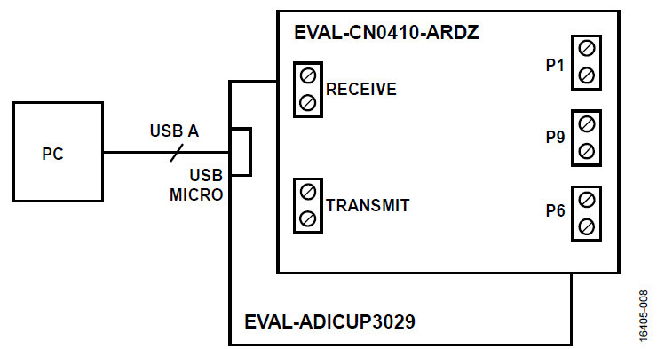
This circuit uses the EVAL-CN0410-ARDZ circuit board, the CFTL-LED-BAR, and the EVAL-ADICUP3029. The EVAL-CN0410-ARDZ is stacked on top of the EVAL-ADICUP3029 using the Arduino-compatible pins.
Equipment Needed
- PC with a USB port and Windows® 7 or above
- EVAL-CN0410-ARDZ circuit evaluation board
- CFTL-LED-BAR evaluation board
- ADICUP3029 evaluation platform or equivalent interface
- CrossCore Embedded Studios (IDE)
- Power supply: 9 V to 19.2 V wall wart
Getting Started
Load the sample code onto the CrossCore Embedded Studios IDE by following the instructions in the Quick Start User Guide.
Functional Block Diagram
Figure 8 shows the functional block diagram of the test setup.
Setup
Connect the EVAL-CN0410-ARDZ by mounting it on top of the EVAL-ADICUP3029 board using the Arduino-compatible headers with their corresponding headers, as shown in Table 1.
| EVAL-CN0410-ARDZ | ADICUP3029 |
| DIGI 1 | P6 |
| DIGI 1 | P7 |
| POWER | P4 |
| ANALOG | P3 |
| CN-0410 Connector | CFTL-LED-BAR Connector |
| P1.1 | P1.2 |
| P1.2 | P1.1 |
| P6.1 | P5.2 |
| P6.2 | P5.1 |
| P9.1 | P9.2 |
| P9.2 | P9.1 |
Then connect the USB cable from the debug port of the EVAL-ADICUP3029 to the USB port of the PC.
Test
With the sample code built and loaded onto the EVAL-ADICUP3029, and the EVAL-CN0410-ARDZ mounted on top with the CFTL-LED-BAR connected, the device communicates with the PC, and codes can now be written to the device via the UART. The circuit can be tested by varying the code written to the board to alter the intensity of the LEDs.
For complete information and details regarding test setup and how to use the software and hardware combined, refer to the CN-0410 User Guide.
More information regarding the EVAL-ADICUP3029 board is available in the EVAL-ADICUP3029 User Guide.
