DN199 : 低成本、高效移动CPU电源
LTC1735是凌力尔特第三代同步降压控制器的最新成员,采用与行业标准LTC1435/LTC1437控制器相同的恒定频率、电流模式架构和突发工作模式(Burst Mode®),并且增强了一些性能。凭借OPTI-LOOP®补偿、新型保护电路、更严格的负载调整和更强大的MOSFET驱动器,LTC1735成为当前和未来几代移动CPU的理想选择。同类器件 LTC1736除具备LTC1735的所有特性之外,还支持符合英特尔移动处理器规范的5位VID电压编程。
LTC1735与上一代控制器LTC1435/LTC1435A引脚兼容,仅外部元件值有微小变化。新的保护特性包括内部折返 限流、输出过压短路保护和可选短路关断。0.8V基准电压支持未来微处理器所需的低输出电压和1%精度。恒定工作频率(可同步至最高500kHz)由外部电容COSC设置,从而为效率优化提供极大的灵活性。
LTC1735的OPTI-LOOP补偿消除了其他控制器对 COUT施加的限制(例如ESR必须非常低),以确保正常运行。99%的最大占空比限制能够支持低压差操作,从而延长电池供电系统的运行时间。同时LTC1735可在3.5V至30V(最高36V)的宽输入电源电压范围内稳定工作。
适用于Pentium® III 处理器的低成本动态VID
图1所示电路从5V至26V的输入电压产生CPU电源(1.6V、10A)。添加图1插图所示的低成本元件,可产生动态 VID两电平输出电压。此实施方案在VG为低电平时产生1.3V的输出电压,在VG为高电平时产生1.5V的输出电压。 LTC1735的过压保护功能可根据设定的输出电压进行动态调整,确保CPU始终受到保护。如果需要“电源良好” 输出,可以用功能增强型器件LTC1735-1取代LTC1735。

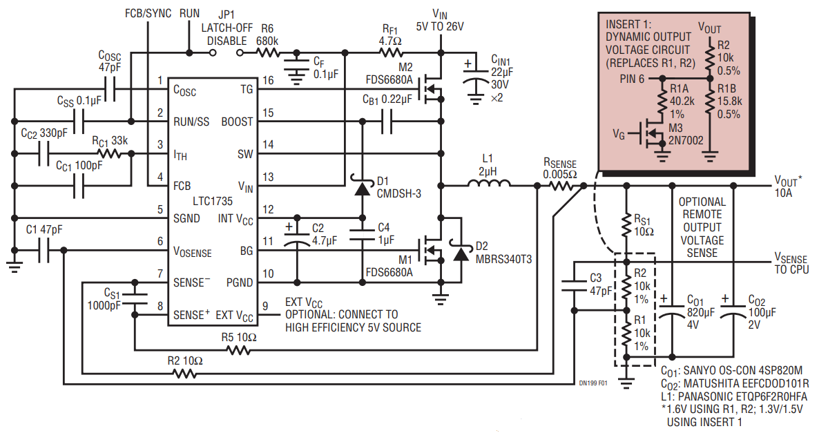
图1. 移动端CPU供电
RUN/SS电容器CSS(见图1)最初用于开启和限制控制器的冲击电流,或是用作短路定时器。如果CSS充电后输出 电压降至标称输出电压的70%以下,则认为输出处于严重过流和/或短路状态,CSS开始放电。如果该状况持续 足够长的时间(由CSS的大小决定),控制器将关断,直到RUN/SS引脚电压重新加载才恢复运行。跳线JP1可禁 用过流闩锁特性。
LTC1735控制器的新增内部保护特性包括折返限流、短路检测、短路闩锁和过压保护。这些特性可保护PC板、MOSFET和CPU免受故障影响。
为什么要禁用过流闩锁?在设计的原型阶段,可能会出现噪声拾取或布局不佳问题,导致保护电路锁定。禁用此特性可以更方便地对电路和PCB布局进行故障排查。内部短路检测和折返限流特性将保持激活,从而保护电源系统免受故障影响。设计完成后,开发者可以决定是否启用闩锁特性。

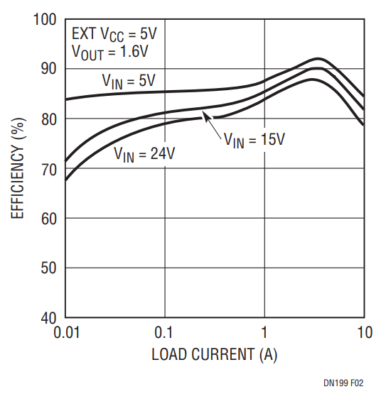
图2. 图1电源的效率
LTC1735电流比较器支持的最大MOSFET电流为75mV/RSENSE。使用低损耗检测电阻不仅能够保证准确限流,而且允许使用低ESR的输出电容,以实现出色的负载阶跃响应。0.005Ω检测电阻可设置最大10A的负载电流(降低RSENSE可设置更高的电流)。LTC1735具有电流折返特性,有助于在输出短接到地时进一步限制负载电流。如果输出下降超过一半,最大检测电压就会降低,以限制底部MOSFET的功耗,使得短路电流为3.5A。请注意,此功能始终激活,且与短路闩锁无关。
FCB引脚是一个多功能引脚,可控制同步MOSFET的操作。它是外部时钟同步的输入,可通过禁用突发工作模式来降低噪声和射频干扰。当FCB引脚电压降至0.8V阈值以下时(FCB = 0V),器件强制进入连续工作模式。在这种情况下,无论主输出端的负载如何,顶部和底部MOSFET都会继续同步驱动。
工作频率由 COSC设置为270kHz。将至少1.5VP-P的时钟信号施加于FCB引脚,LTC1735的内部振荡器便可与外部振荡器同步。当与外部频率同步时,突发工作模式被禁用,但由于电流反向受到抑制,在低负载电流下会发生周期跳过现象。底部栅极每10个时钟周期导通一次,确保自举电容保持刷新,并将频率保持在音频范围之上。当外部时钟的上升沿施加到FCB引脚时,即触发一个新的周期。 COSC = 47pF时,同步范围为240kHz至400kHz。
LTC1735采用新的“软闩锁”OVP电路。无论工作模式如何,只要输出电压超过稳压点7.5%以上,同步MOSFET就会强制导通。然而,如果电压随后恢复到安全水平,器件就可以恢复正常运行,从而防止噪声或电压重新编程导致闩锁。这在动态改变输出电压时很重要,因为过压保护阈值会随着新输出电压而调整,确保CPU始终受到保护。
先前的过压闩锁保护方案存在许多问题。其中最突出、也是最棘手的问题之一,是噪声或瞬态信号在极短时间内超过OVP阈值,导致误断路。每次发生这种OVP闩锁时,都需要手动复位来重新启动稳压器。
相比LTC1435系列,LTC1735可用于具有更高电流的应用。更强的栅极驱动支持并联多个MOSFET或在更高频率 下运行。LTC1735已针对低输出电压操作进行了优化,将最短导通时间缩减至200ns以下。但请记住,在高输入电压和高频率下,转换损耗仍然会严重影响效率。LTC1735确实能够在300kHz以上的频率工作,但这未必是最佳做法。
作者
