AN-42: Voltage Reference Circuit Collection
This application note is a guidebook of circuits featuring voltage reference ICs in various configurations. The circuits shown are both basic as well as complex and employ many popular IC references. Included are 2-terminal and 3-terminal references in series and shunt modes, for positive and negative polarities, in voltage and current boosted versions. Additional circuit information can be located in the references listed in the index. The reference works as follows, i.e., AN8, page 2 = Application Note 8, page 2; LTC1044 DS = LTC1044 data sheet.
| VOLTAGE VZ (VOLTS) | VOLTAGE TOLERANCE MAXIMUM TA = 25°C | DEVICE | TEMPERATURE DRIFT, ppm/°C OR mV CHANGE | OPERATING CURRENT RANGE (OR SUPPLY CURRENT) | MAXIMUM DYNAMIC IMPEDANCE (Ω) | MAJOR FEATURE |
| 1.235 |
± 0.32% ± 0.32% ± 1% ± 1% ± 2% ± 1% |
LT1004C-1.2 LT1004CS8-1.2 LT1034BC-1.2 LT1034C-1.2 LM385-1.2 LM385B-1.2 |
20ppm (typ) 20ppm (typ) 20ppm (max) 40ppm (max) 20ppm (typ) 20ppm (typ) |
10μA to 20mA 10μA to 20mA 20μA to 20mA 20μA to 20mA 15μA to 20mA 15μA to 20mA |
1.5 1.5 1.5 1.5 1.5 1.5 |
Micropower Micropower Low TC Micropower with 7V Aux. Reference Low TC Micropower with 7V Aux. Reference Micropower Micropower |
| 2.5 |
± 0.5% ± 0.8% ± 0.2% ± 2.5% ± 0.2% ± 4% ± 2% ± 3% ± 1.5% ± 3% ± 1% ± 0.4% ± 0.4% |
LT1004C-2.5 LT1004CS8-2.5 LT1009C LT1009S8 LT1019C-2.5 LM336-2.5 LM336B-2.5 LM385-2.5 LM385B-2.5 LM580J LM580K LM580L LM580M |
20ppm (typ) 20ppm (typ) 6mV (max) 25ppm (max) 20ppm (max) 6mV (max) 6mV (max) 20ppm (typ) 20ppm (typ) 85 (max) 40 (max) 25 (max) 10 (max) |
20μA to 20mA 20μA to 30mA 400μA to 10mA 400μA to 20mA 1.2mA 400μA to 10mA 400μA to 10mA 20μA to 20mA 20μA to 20mA 1.5mA 1.5mA 1.5mA 1.5mA |
1.5 1.5 1.4 0.6 N/A 1.4 1.4 1.5 1.5 N/A N/A N/A N/A |
Micropower Micropower Precision Precision Precision Bandgap General Purpose General Purpose Micropower Micropower 3 Terminal Low Drift 3 Terminal Low Drift 3 Terminal Low Drift 3 Terminal Low Drift |
| 4.5 |
± 0.2% |
LT1019C-4.5 |
20ppm (max) |
1.2mA |
N/A |
Precision Bandgap |
| 5.0 |
± 0.2% ± 1% ± 0.05% ± 1% ± 1% ± 0.02% ± 0.05% ± 0.05% ± 0.05% ± 0.1% ± 0.2% ± 1% ± 0.3% ± 0.5% ± 1% ± 2% |
LT1019C-5 LT1021BC-5 LT1021CC-5 LT1021DC-5 LT1021CS8 LT1027A LT1027B LT1027C LT1027D LT1027E LT1029AC LT1029C REF02E REF02H REF02C REF02E |
20ppm (max) 5ppm (max) 20ppm (max) 20ppm (max) 20ppm (max) 2ppm (max) 2ppm (max) 3ppm (max) 5ppm (max) 7.5ppm (max) 20ppm (max) 34ppm (max) 8.5ppm (max) 25ppm (max) 6.5ppm (max) 250ppm (max) |
1.2mA 1.2mA 1.2mA 1.2mA 1.2mA 2.0mA 2.0mA 2.0mA 2.0mA 2.0mA 700μA to 10mA 700μA to 10mA 1.4mA 1.4mA 1.6mA 2.0mA |
N/A 0.1 0.1 0.1 0.1 N/A N/A N/A N/A N/A 0.6 0.6 N/A N/A N/A N/A |
Precision Bandgap Very Low Drift Very Tight Initial Tolerance Low Cost, High Performance Low Cost, High Performance Low Drift, Tight Tolerance Low Drift, Tight Tolerance Low Drift, Tight Tolerance Low Drift, Tight Tolerance Low Drift, Tight Tolerance Precision Bandgap Precision Bandgap Precision Bandgap Precision Bandgap Precision Bandgap Bandgap |
| 6.9 |
± 3% ± 5% ± 5% ± 5% ± 4% |
LM329A LM329B LM329C LM329D LTZ1000 |
10ppm (max) 20ppm (max) 50ppm (max) 100ppm (max) 0.1ppm/°C |
600μA to 15mA 600μA to 15mA 600μA to 15mA 600μA to 15mA 4mA |
0.1 (typ) 0.1 (typ) 0.1 (typ) 0.1 (typ) 20.0 |
Low Drift Low Drift General Purpose General Purpose Ultra Low Drift, 2ppm Long Term Stability** |
| 6.95 |
± 5% ± 5% |
LM399 LM399A |
2ppm (max) 1ppm (max) |
500μA to 10mA 500μA to 10mA |
1.5 1.5 |
Ultra Low Drift Ultra Low Drift |
| 7.0 |
± 0.7% ± 0.7% |
LT1021BC-7 LT1021DC-7 |
5ppm (max) 20ppm (max) |
1.0mA 1.0mA |
0.2 0.2 |
Low Drift/Noise, Exc. Stability Low Cost, High Performance |
| 10.0 |
± 0.2% ± 0.5% ± 0.05% ± 0.5% ± 0.5% ± 0.1% ± 0.2% ± 0.3% ± 0.1% ± 0.3% ± 0.5% ± 1% |
LT1019C-10 LT1021BC-10 LT1021CC-10 LT1021DC-10 LT1031BC LT1031CC LT1031DC LT581J LT581K REF01E REF01H REF01C |
20ppm (max) 5ppm (max) 20ppm (max) 20ppm (max) 5ppm (max) 15ppm (max) 25ppm (max) 30ppm (max) 15ppm (max) 8.5ppm (max) 25ppm (max) 65ppm (max) |
1.2mA 1.7mA 1.7mA 1.7mA 1.7mA 1.7mA 1.7mA 1.0mA 1.0mA 1.4mA 1.4mA 1.6mA |
N/A 0.25 0.25 0.25 0.25 0.25 0.25 N/A N/A N/A N/A N/A |
Precision Bandgap Very Low Drift Very Tight Initial Tolerance Low Cost, High Performance Very Low Drift Very Tight Initial Tolerance Low Cost, High Performance 3 Terminal Low Drift 3 Terminal Low Drift Precision Bandgap Precision Bandgap Precision Bandgap |
| * COMMERCIAL 0°C to + 70°C ** LTZ1000 requires external control and biasing circuits. |
||||||
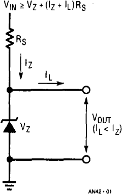
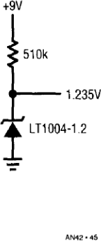
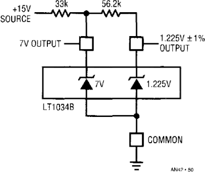
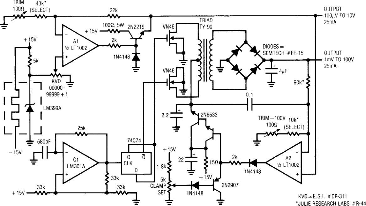
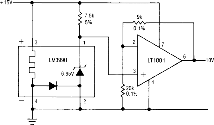
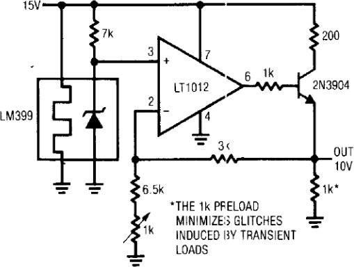
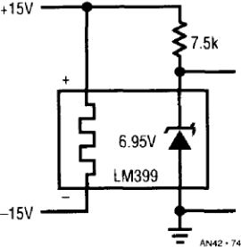
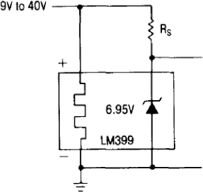
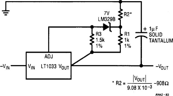
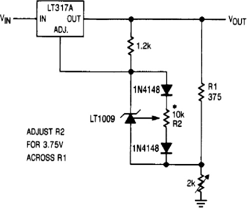
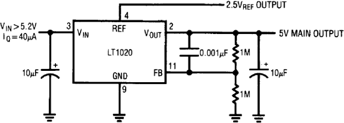
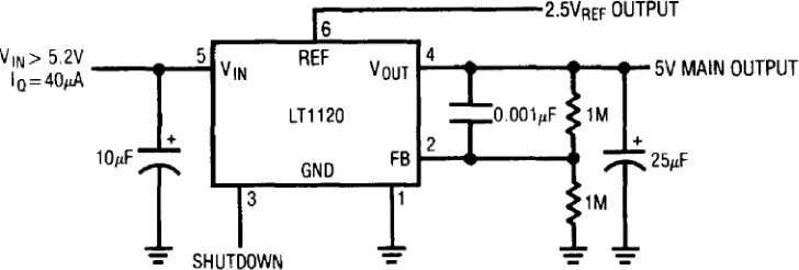
Figure 1. Basic Operation of Shunt Reference Family.
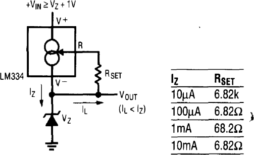
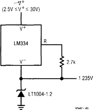
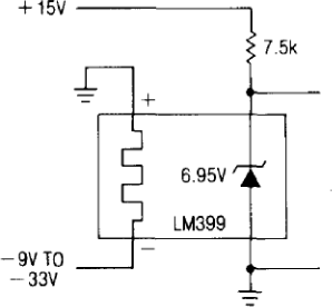
Figure 2. Current Source Stabilized Reference.
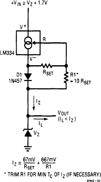
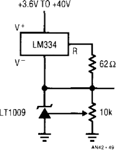
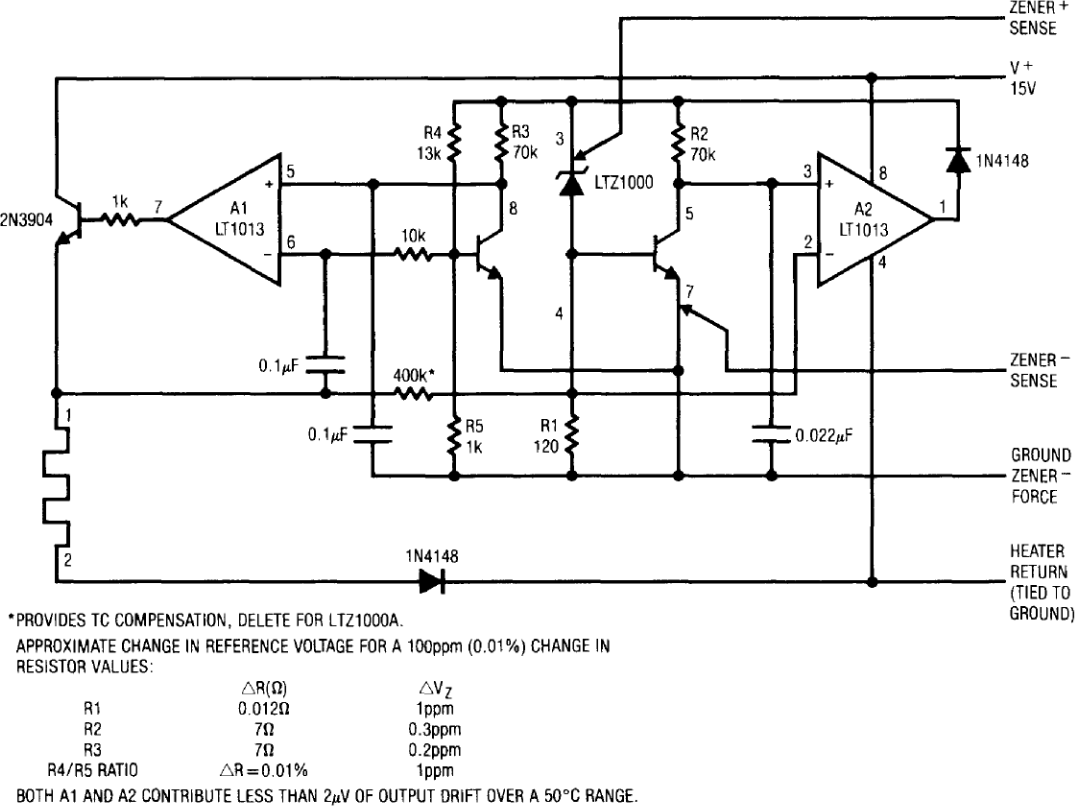
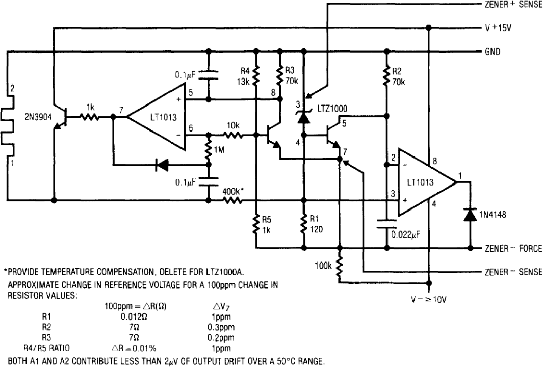
Figure 3. Low TC Current Stabilized Reference.
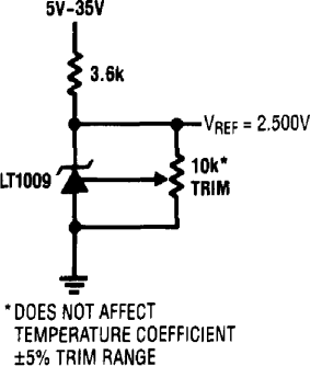
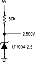
Figure 4. 2.5V Output Reference, ±5% Trim Range.
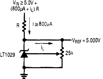
Figure 5. 5V Output Reference, +5%, –13% Trim Range.
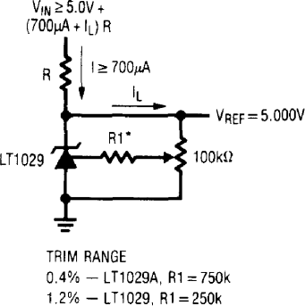
Figure 6. 5V Output Reference, Narrow Trim Range.
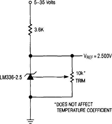
Figure 7. 2.5V Output, Temperature Independent Trim.
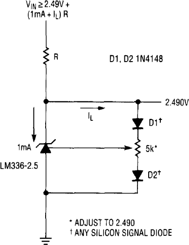
Figure 8. 2.490V Output, Trim for Minimum TC.

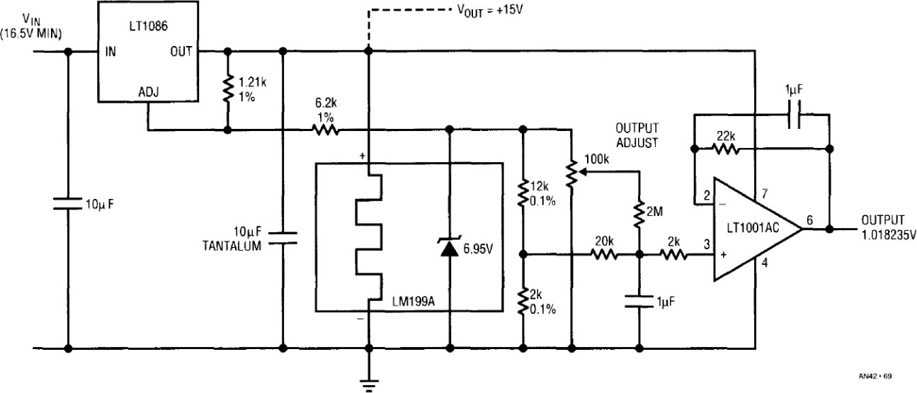
Figure 9. 5.120V Output, Trimmed Reference.
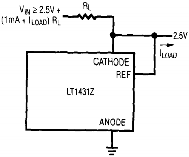

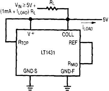
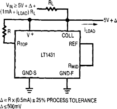
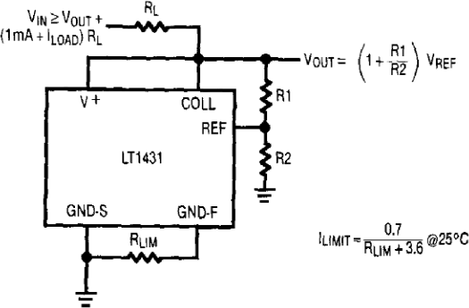
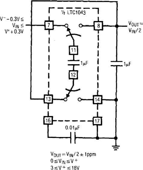
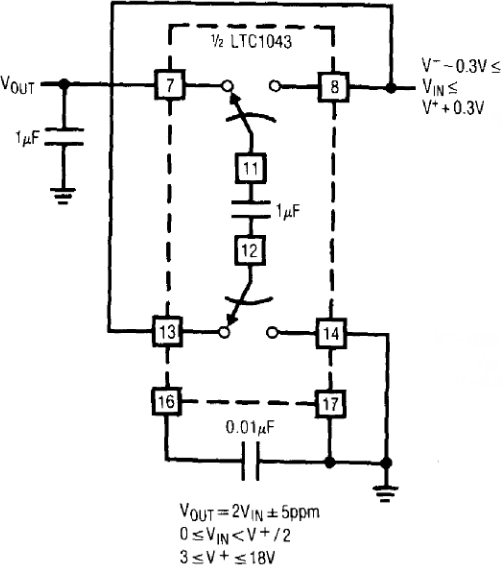
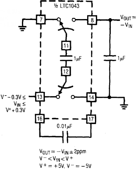
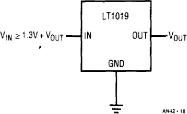
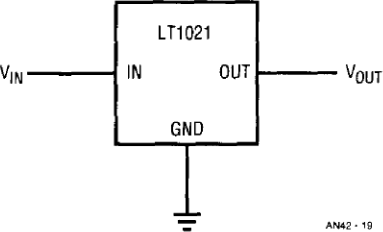
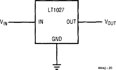
Figure 20. Basic Hookup for LT1027 Series Reference.
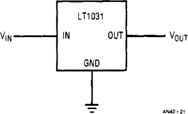
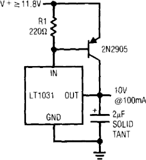
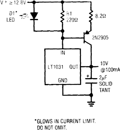
Figure 21. Basic Hookup for LT1031 Series Reference.
| LT1031 PERFORMANCE | ||
| DEVICE | VOUT | TC IN ppm/°C (TYP/MAX) |
| LT1031B | 10V ±5mV | 3/5 |
| LT1031C | 10V ±10mV | 6/15 |
| LT1031D | 10V ±20mV | 10/25 |
| LT1021 PERFORMANCE | ||
| DEVICE | VOUT | TC IN ppm/°C (TYP/MAX) |
| LT1021C-5 | 5V ±2.5mV | 3/20 |
| LT1021B-5 | 5V ±50mV | 2/5 |
| LT1021B-7 | 7V ±50mV | 2/5 |
| LT1021D-7 | 7V ±50mV | 3/20 |
| LT1021C-10 | 10V ±5mV | 5/20 |
| LT1021B-10 | 10V ±50mV | 2/5 |
| LT1019 PERFORMANCE | ||
| DEVICE | VOUT | TC IN ppm/°C (TYP/MAX); C =COM, M = MIL |
| LT1019A-2.5 | 2.5V ±1.25mV | 3/5 (C), 5/10 (M) |
| LT1019-2.5 | 2.5V ±5mV | 5/20 (C), 8/25 (M) |
| LT1019A-5 | 5V ±2.5mV | 3/5 (C), 5/10 (M) |
| LT1019-5 | 5V ±10mV | 5/20 (C), 8/25 (M) |
| LT1019A-10 | 10V ±5mV | 3/5 (C), 5/10 (M) |
| LT1019-10 | 10V ±20mV | 5/20 (C), 8/25 (M) |
| LT1027 PERFORMANCE | ||
| DEVICE | VOUT | TC IN ppm/°C (TYP/MAX) |
| LT1027A | 5V ±1mV | 1/2 |
| LT1027B | 5V ±2.5mV | 1/2 |
| LT1027C | 5V ±2.5mV | 2/3 |
| LT1027D | 5V ±2.5mV | 3/5 |
| LT1027E | 5V ±5mV | 5/7.5 |
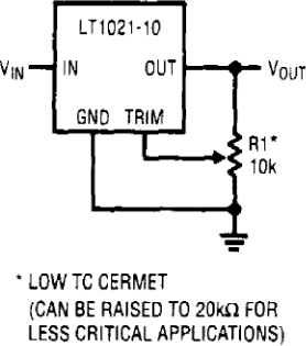
Figure 22. 10V Output, Full Trim Range (±0.7%).
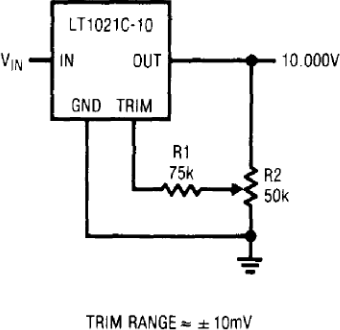
Figure 23. 10V Output, Restricted Trim Range for Improved Resolution.
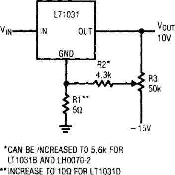
Figure 24. 10V Output, Trimmed Reference.
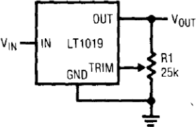
Figure 25. Wide Trim Range (±5%).
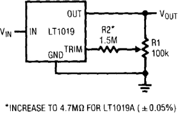
Figure 26. Narrow Trim Range (±0.2%).
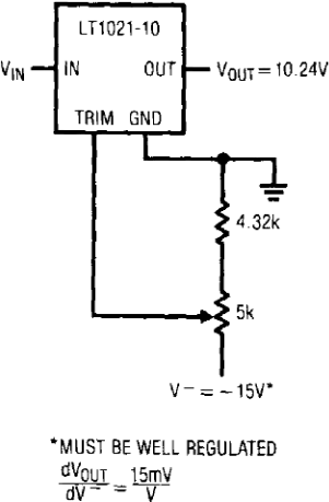
Figure 27. 10V Output, Trimmed to 10.24V.
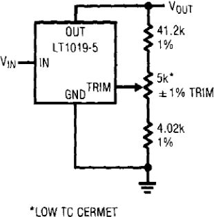
Figure 28. 5V Output, Trimmed to 5.120V.
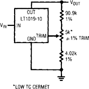
Figure 29. 10V Output, Trimmed to 10.240V.
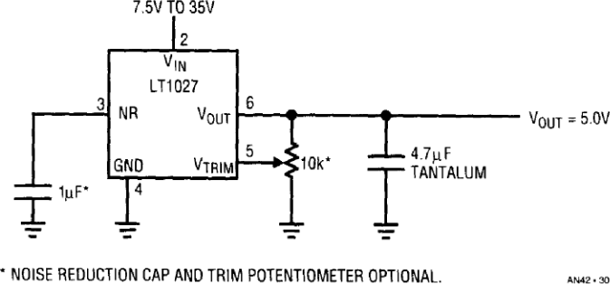
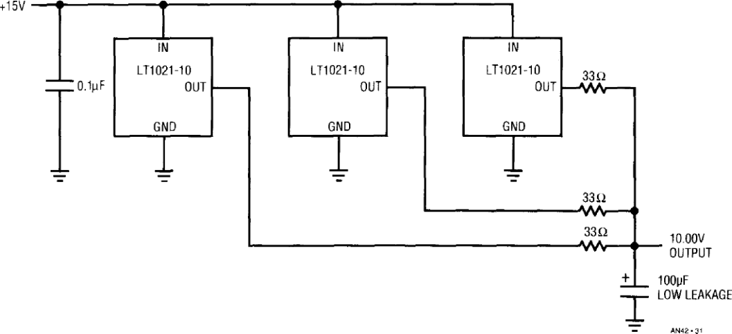

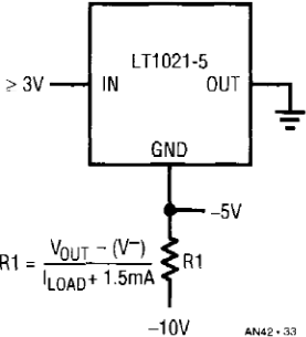
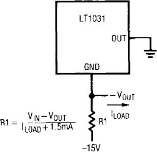




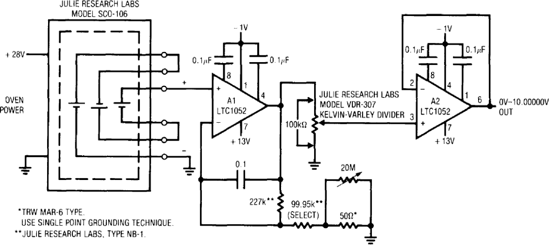
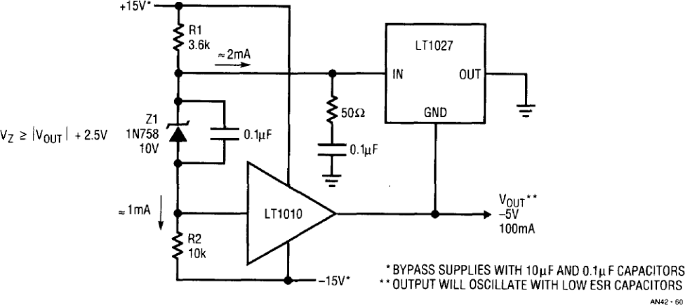
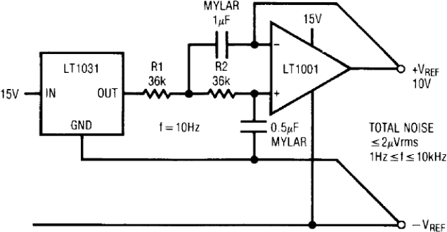
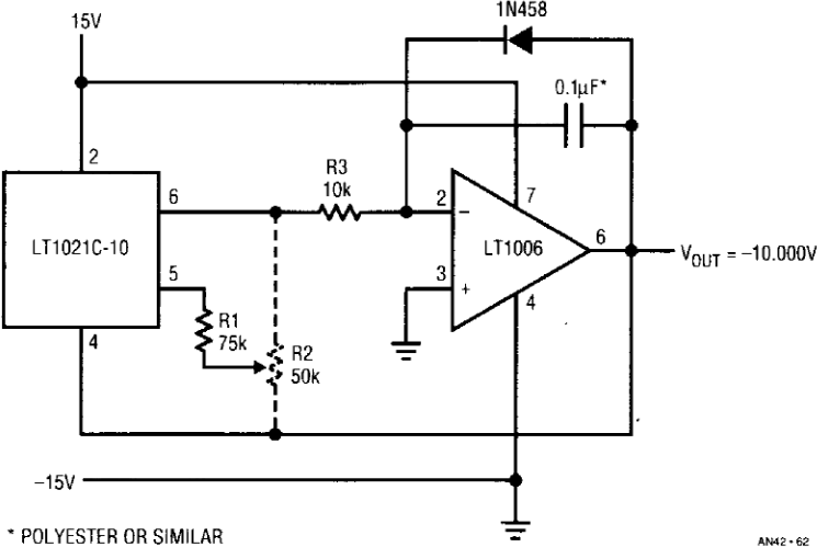


Appendix A
Precision Resistor Selection
Resistors are commonly used in precision linear circuits. Common precision resistor technologies include thin-film; thick-film, metal foil, and wirewound. Selecting the appropriate resistor type for a given application requires some understanding of the capabilities of the various devices available.
In many applications resistor selection depends on resistance value, absolute accuracy, and power dissipation. However, when designing precision linear circuits other performance parameters usually must be considered. These include temperature coefficient, load life stability, and voltage coefficient. The relative importance of any parameter depends on the particular application. Table A1 lists characteristics of different resistor types. Because individual processes vary, characteristics for the same resistor technology vary between manufactures.
| CHARACTERISTIC | CARBON COMPOSITION | THIN-FILM CARBON FILM | THICK-FILM CERMET | THIN-FILM MiCr FILM | WIREWOUND | METAL FOIL (MOLDED) | METAL FOIL (HERMETIC) | |
| Ohmic Range | 2.7M-100M | 1M-4.7M | 1M-3M | 10M-3M | 20k-468k | 1k-250k | 1k-250k | |
| Absolute Accuracy* | Standard Available | 5% 20%-5% |
5.0% | 1.0% 5.0%-0.1% |
0.1% 1.0%-0.01% |
0.01% 1.0%-0.005% |
0.01% 1.0%-0.005% |
0.01% 1.0%-0.001% |
| Temperature Coefficient* | Standard Available | – 5000ppm/°C | – 200ppm/°C – 100ppm/°C-–1500ppm/°C |
100ppm/°C 25ppm/°C-200ppm/°C |
10ppm/°C 15ppm/°C-25ppm/°C |
5ppm/°C 1.0ppm/°C-20ppm/°C |
2.5ppm/°C-8ppm/°C | 0.6ppm°C |
| TCR Tracking* | 1: (1-9), 1.0ppm/°C 1: (10-100), 2.0ppm/°C 1: (100-1000), 4.0ppm/°C |
1: (1-4), 0.5ppm/°C 1: (5-10), 2.0ppm/°C |
1: (1-4), 0.5ppm/°C 1: (5-10), 1.0ppm/°C |
1: (1-4), 0.5ppm/°C 1: (5-10), 1.0ppm/°C |
||||
| Ratio Matching* | 1: (1-9), 0.005% 1: (10-100), 0.01% 1: (100-1000), 0.02% |
1: (1-4), 0.005% 1: (5-10), 0.1% |
(1-4), 0.005% 1: (5-10), 0.1% |
(1-4), 0.005% 1: (5-10), 0.1% |
||||
| Load-Life Stability* | 1kHRS, 6% – 4% |
3.0% | 1.0% | 1kHRS, 0.02% | 10kHRS, 0.2% | 2kHRS, 0.015% 10kHRS, 0.05% |
2kHRS, 0.015% | |
| Shelf-Life* | 2.0% | 0.1% | 30ppm/YR | 100ppm/YR | 25ppm/YR | 5ppm/YR | ||
| Voltage Coefficient Of Resistance | – 0.02%/V | 0.05ppm/V | 0.1ppm/V | 0.1ppm/V | 0.1ppm/V | |||
| Resistor Classification | General Purpose | General Purpose | Semi-Purpose | Precision | Precision | Ultra-Precision | Ultra-Precision | |
| Manufacturer's Part Number | Allen-Bradley** CB Series |
International** Resistive Co. |
International** Resistive Co. |
International** Resistive Co. MAR5 |
Vishay/Ultronix** 105A |
Vishay** S102 Series |
Vishay** VHP1000 |
|
| * ±Unless otherwise stated ** Parameters may vary between manufacturers % = ppm × 0.0001 0.0001% = 1ppm 0.001% = 10ppm 0.01% = 100ppm 0.1% = 1000ppm 1% = 10000ppm |
||||||||
Package type can significantly influence stability. Some packages more effectively protect the resistive element from stresses due to handling, packaging, insertion, and lead forming. Also, manufacturing conditions including solder baths, cleaning solutions, and humidity can cause shifts in a resistor’s value. Common package choices include conformal coating, molded and hermetic types. Conformal coated parts are the most common types in semi-precision applications. Hermetic sealing offers substantial stability improvements, regardless of resistor technology. Hermetically sealed metal cases also provide electrostatic shielding and isolation from humidity and other environmental effects.
Ultra-stable time and temperature characteristics become an issue when circuitry must hold calibration over extended ranges of time and temperature. In these applications an oil filled package may be required. The oil integrates ambient temperature variations, preventing thermal gradients across the resistor.
Various technologies available offer a spectrum of price-performance tradeoffs. Because of this, a summary of resistor types is useful.
Thin-Film
In the thin-film process, typically metal film, Nickel-Chromium (Nichrome) or Tantalum-Nitride is deposited on a ceramic substrate by evaporation or sputtering techniques. The sputtering process is preferred since it produces a more stable device. The 750Å-1500Å film can be applied to either a planar substrate or a ceramic cylindrical core. Resistor networks use the planar substrate with discrete thin-film resistors utilizing the familiar cylindrical shape. Nichrome parts have typical temperature coefficient of resistance (TCR) of 25ppm/°C for a planar substrate and 50ppm/°C for a ceramic core substrate. Tantalum-Nitride resistors tend to be slightly higher.
Bulk-Metal Foil
Buck-metal foil resistors are made with a Nickel-Chromium alloy that is cemented to a planar ceramic substrate. The Nichrome alloy, substrate, and adhesive material are carefully balanced to achieve an overall low temperature sensitivity. The bulk-metal foil’s 25,000Å thickness is significantly less susceptible to humidity than thin-film types.
Bulk-metal foil resistors are ultra-precision components. Generally, they offer tighter tolerance, better stability, and lower TCR’s than their thin-film counterparts. Their high stability and uniformity makes them a good candidate for precision networks. The networks use hybrid type construction and offer extraordinary ratio stabilities (0.5ppm/°C). Unfortunately, bulk-metal technologies may cost two to five times that of film resistors.
Wirewound
Wirewound resistors are usually made by winding resistive wire of a specific diameter characteristic around a core or card. Performance depends on the alloy used, wire lengths, diameter, and annealing process. Wirewound resistors can be ultra-precision components and are best suited in applications that require absolute accuracy, stability, power, or low resistance value. Wirewounds have excellent overload handling capability, but are poor candidates for high speed work due to inductive effects. Special winding schemes can greatly reduce this parasitic inductance, but never entirely eliminate it.
Thick-film
Thick-film resistors are made from a paste mixture of Metal-Oxide (cermet) and binder particles, screen printed onto a ceramic substrate and fired at high temperatures. They are semi-precision components, with standard 1% tolerance and typical TC’s of 100ppm/°C to 200ppm/°C.
Carbon Composition/Carbon Film
Carbon composition resistors are made from a large chunk of resistive material. They can handle large overloads for a short period of time. This is their main advantage over the other resistor technologies. They are general purpose components, not precision. Carbon composition resistors do not have constant TC’s. TC’s can vary anywhere between –2000ppm/°C to –8,000ppm/°C and have shelf-life stabilities of 2% to 5% of resistance value (20,000ppm/Yr to 50,000ppm/Yr ).
Carbon film resistors are manufactured using a thin-film process. Initial tolerance and TC are similar to carbon composition. However, they do not have the high overload capability. The sole advantage is their low cost.
Resistor Manufacturers
- Vishay/Ultronix
461 North 22nd Street
P.O. Box 1090
Grand Junction, CO 81502
(303) 242-0810 - Vishay Resistive Systems Group
63 Lincoln Highway
Malvern, PA 19355
(215) 644-1300 - International Resistive Company
P.O. Box 1860
Boone, NC 28607
(704) 264-8861 - Julie Research Laboratories
508 West 26th Street
New York, NY 10001
(212) 633-6625 - Allen-Bradley Company, Inc.
Electronic Components Division
1414 Allen-Bradley Drive
El Paso, TX 79936-4888
(800) 592-4888
Appendix B
Capacitor Selection
Capacitor Selection for voltage reference circuitry requires care. Capacitor parasitics can introduce errors. Typical capacitors found in reference circuitry include aluminum and tantalum electrolytics, ceramic, and polyester. Table B1 summarizes characteristics pertinent to reference applications. It reveals that equivalent value capacitors have electrical characteristics that vary widely between different capacitor technologies.
| CHARACTERISTIC | ALUMINUM SOLID ELECTROLYTIC | POLYESTER FILM | SOLID TANTALUM ELECTROLYTIC | MULTILAYER CERAMIC | ALUMINUM ELECTROLYTIC | UNIT |
| Capacitance | 0.47 | 0.47 | 0.47 | 0.47 | 0.47 | μF |
| ESR* 100kHz | 0.198 | 0.456 | 4.5 | 0.062 | 5.4 | Ω |
| Leakage Current* @ 5V | 20 | 0.03 | 30 | 0.16 | 175 | nA |
| Manufacturer's | SANYO | SANYO | KEMET | KEMET | SANYO | |
| *Typical | ||||||
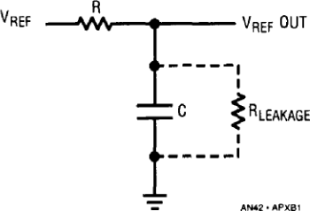
Leakage current becomes an issue when an RC network filters a reference voltage. The leakage combines with the resistor to shift the output voltage. Leakage varies with time and temperature and varies from device to device. A low leakage capacitor must be used in these applications. The problem is illustrated by considering Figure B1. With R = 1M, 1x10–12 leakage path in a capacitor creates a 1ppm error. Figure B2 is another approach to minimizing leakage induced errors. Here, the voltage across C1 is reduced to zero by bootstrapping via R1. Under these conditions C1’s leakage current is effectively zero since there is 0V across it. C2’s leakage appears in series with R1, rendering it harmless.

Output capacitors provide low output impedance at high frequencies. Large capacitors at the output of some references may cause oscillations. The capacitor introduces a feedback pole which reduces phase margin of the reference. Phase shift can be excessive with low effective series resistance (ESR) capacitors. The phase shift can be reduced by placing a small value resistor in series with the capacitor. If the phase shift is significant the reference will ring during transient conditions or simply oscillate. This condition is particularly significant for SAR type A/D converter applications. Here, the reference output must settle quickly or conversion errors will result. Consult manufacturers data sheet for recommended output by passing techniques. Also, all references are not stable with all capacitive loads.
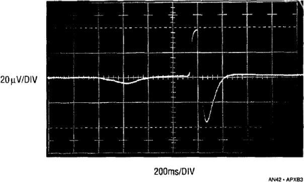
Leakage and AC effects are not the only sources of problems. Some ceramic capacitors have a piezoelectric response. A piezoelectric device generates a voltage across it’s terminals due to mechanical stress, similar to the way a piezoelectric accelerometer or microphone works. For a ceramic capacitor the stress can be induced by vibrations in the system or thermal transients. The resulting voltages produced can cause appreciable reference errors. A ceramic capacitor produced Figure B3’s trace in response to light tapping from a pencil. Similar vibration induced behavior can masquerade as reference instabilities.
Capacitor Manufacturers
- Nichicon (America) Corporation
927 East State Parkway
Schaumburg, IL 60195
(708) 843-7500 - Sanyo Video Components (USA) Corporation
1201 Sanyo Avenue
San Diego, CA 92073
(619) 661-6322 - United Chemi-Con, Inc.
9801 West Higgins Road
Rosemount, IL 60018
(312) 696-2000 - Illinois Capacitor, Inc.
3757 West Touhy Avenue
Lincolnwood, IL 60645
(312) 675-1760 - Kemet Electronics
P.O. Box 5928
Greenville, SC 29606
(803) 963-6300
Appendix C
Trimming Techniques
It is often necessary to adjust a resistor’s value in precision circuits. The desired value may not be available or readily predictable. Either case necessitates a trim.
For optimum stability and adjustability, always use the smallest value of trim resistance that gives the required range of adjustment. The reduces the stability and drift due to the poor matching characteristics between the fixed resistor and trim resistor. There seems to be a tendency for designers to use a 0.01% resistor with a 1% trim adjustment. Don’t pay for accuracy that isn’t needed.
Avoid the extremes of resistance range when using a trimmer. Although the entire range will meet the stated specifications, mid-range values tend to perform (TC, tracking, etc.) better than low and high values.
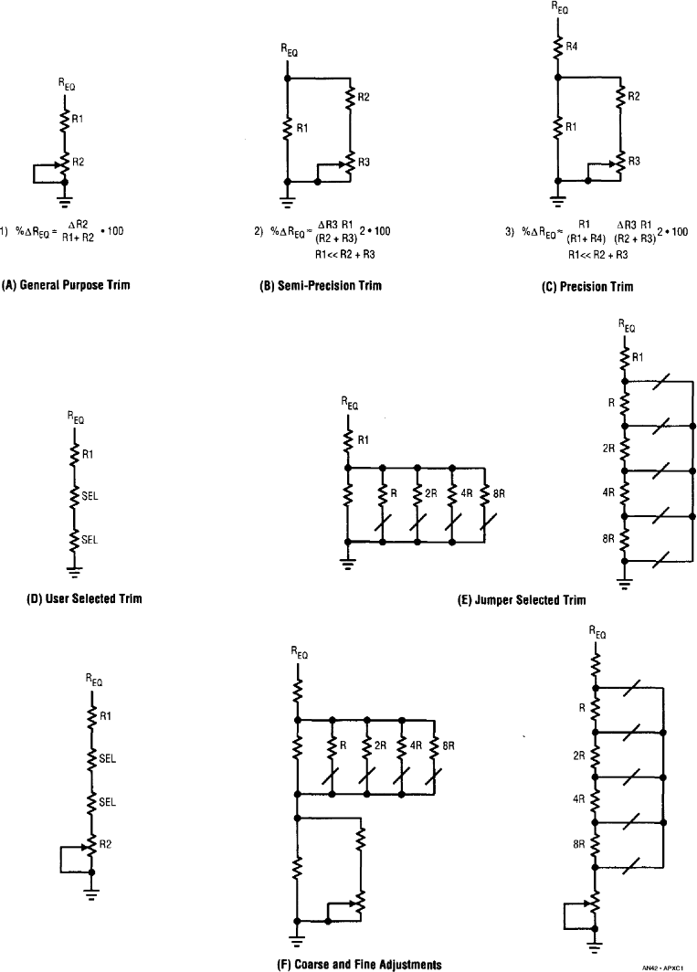
Typical resistor trimming techniques are shown in Figure C1. Selecting the appropriate method depends on various factors including trim range, temperature stability, long term stability, manufacturing processes, and calibration procedures. Figure C1(A) is a general purpose trim. This technique has an extremely wide range. Equation 1 represents the percentage change in the desired resistor value, REQ, for a change in trim resistance. This equation is useful when determining the optimum trimmer resistance and is provided for the various trimming schemes. If increased stability is required, the circuit in Figure C1(B) can be used. In this case, increased stability is achieved at the expense of a narrower trim range. R1 must have a tighter absolute tolerance than in the previous circuit for this technique to be useful. For improved resolution, a resistor can be placed in series with this network, see Figure C1(C). This approach is best suited for ultra-precision applications, since it has the highest resolution.
In some applications potentiometers may be unreliable. In these cases, resistor value can be trimmed by selecting the appropriate series resistor value, see Figure C1(D). However, this requires numerous resistors that must be hand picked in production. An alternative approach is to use a binary weighted trim as Figure C1(E). The resistance is trimmed by opening various links. With just four resistors there are 16 different resistor values possible.
With this method, the need for a bin of resistors on the production floor is eliminated.
Often, the best solution is to have coarse and fine adjustments. This can provide a more stable resistor value. Figure C1(F) illustrates various ways to implement this approach.
In many voltage reference circuits it is necessary to scale and buffer the output of a reference to some calibrated voltage. The trim sets the output voltage to the desired degree of accuracy. Figure C2 shows various techniques for trimming the buffered output. These examples utilize various resistor trimming techniques to set output voltage.
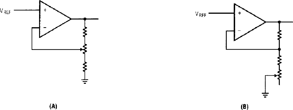
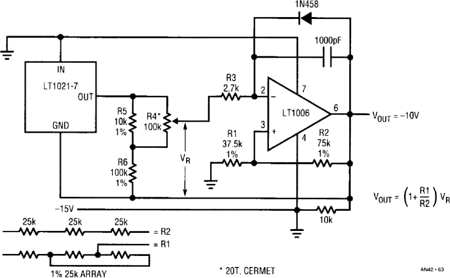
Figure C2 (B) shows a simple voltage reference circuit. The reference is connected to the non-inverting input of an op amp. The feedback resistors around the op amp scale the output voltage to the approximate output voltage. The potentiometer fine tunes the output to the desired value.
The temperature coefficient (TC) of the op amps gain setting resistors can add significant error to the reference output due to ambient temperature changes. The circuits temperature coefficient is primarily set by the ration matching characteristics of the resistors, as opposed to their absolute tolerance. Matched resistor sets provide a decade or greater improvement in tempco performance than individually specified resistors. Therefore, resistors that have relatively high TC’s can be used if they track.
Another interesting characteristic of this circuit is the magnitude if output voltage drift with temperature caused by the gain setting resistors. The drift error contributed by the resistors is determined by multiplying their ratio (R1/R2) by their TCR tracking tolerance. For example, to obtain a 10V output from a 6.9V reference the gain setting resistors ratio needs to be about 0.45. This means that 10ppm/°C resistor TCR tracking effects output voltage by only 4.5ppm/°C. Therefore, for minimum effect of the resistor’s TCR tracking, it is desirable to have the reference voltage be a large percentage of the output voltage.
The remaining circuits in Figure C2 show some alternatives for trimming a reference voltage. The particular circuit selected depends upon the required performance specifications and manufacturing processes.

If reliability is an issue, do not rely on the potentiometer wiper contact. The open wiper condition is a common trimmer failure. If this occurs the outputs in Figure C3 will go to the supply rails, possibly damaging other system components. With the unused portion of the trimmer tied to the wiper (Figure C2 (B2)) the output can only shift by the amount permitted by the total trimmer resistance, improving reliability.
