AD4060
RECOMMENDED FOR NEW DESIGNSCompact, Low Power, 12-Bit, Easy Drive SAR ADC with I3C Interface
- Part Models
- 3
- 1ku List Price
- Starting From $4.90
Overview
- Small footprint, big performance
- INL: ±0.1 LSB maximum
- SNR: 73.8dB with VREF = 3.3V
- 1.35nJ per conversion
- 405μW at 300kSPS in sample mode
- 370μW/112μW at 1MSPS/300kSPS in autonomous modes
- 4.1μW standby power
- Versatile signal conditioning integration
- Easy Drive features enable small, low-power AFE designs
- Compatible with differential and single-ended signal chains
- Wide common-mode input range
- Minimizes digital host activity and power dissipation
- Autonomous sampling with window comparator and interrupt generation
- Averaging filter with burst sampling support
- Power cycling synchronization for companion devices
- 2-wire I3C Interface compatible with 1.8V to 3.3V logic
- 2.00mm × 2.6mm LFCSP and 1.67mm × 1.97mm WLCSP
- Wide operating temperature range: −40°C to +125°C
The AD4060 is a versatile, 12-bit, successive approximation register (SAR) analog-to-digital converter (ADC) that enables low-power, high-density data acquisition solutions without sacrificing precision. This ADC offers a unique balance of performance and power efficiency, plus innovative features for seamlessly switching between high-resolution and low-power modes tailored to the immediate needs of the system. The AD4060 is ideal for battery-powered, compact data acquisition and edge sensing applications.
The Easy Drive features enable highly efficient analog front end (AFE) designs. The small sampling capacitors (3.4pF) maximize input impedance, thus reducing the dependence on high-bandwidth, power-hungry amplifiers typically required by SAR ADCs. The wide input common-mode range grants inherent support for both differential and single-ended signals.
The AD4060 supports microcontrollers with power-down modes and interrupt-driven firmware. The autonomous modes enable out-of-range event detection while the digital host sleeps. The burst averaging mode delivers on-demand, high-resolution measurements while offloading computations from the host processor. The self-timed device enable signal (DEV_EN) synchronizes AFE device power cycling to the ADC sampling instant, optimizing system power consumption while minimizing power-up settling error artifacts. The AD4060 also supports power cycling the voltage reference and using the supply as the ADC reference voltage (VREF) for additional power savings.
The device configuration and ADC data readback is supported via a robust, 2-wire I3C interface with cyclic redundancy check (CRC) supported for all data transfers. The AD4060 is available in compact 14-Lead Lead Frame Chip Scale [LFCSP] and 16-Ball Wafer Level Chip Scale [WLCSP] packages and operates across a wide temperature range, making it ideal for a diverse set of applications.
Applications
- Battery-powered data acquisition
- Vital signs monitoring
- Biological and chemical analysis
- Geologic and seismic sensing
- Motion and robotics
Documentation
Data Sheet 1
User Guide 1
Device Drivers 1
ADI has always placed the highest emphasis on delivering products that meet the maximum levels of quality and reliability. We achieve this by incorporating quality and reliability checks in every scope of product and process design, and in the manufacturing process as well. "Zero defects" for shipped products is always our goal. View our quality and reliability program and certifications for more information.
| Part Model | Pin/Package Drawing | Documentation | CAD Symbols, Footprints, and 3D Models |
|---|---|---|---|
| AD4060BCBZ-RL7 | WLCSP | ||
| AD4060BCPZ-R2 | LFCSP | ||
| AD4060BCPZ-RL7 | LFCSP |
Software Resources
Device Drivers 1
Evaluation Software 1
Can't find the software or driver you need?
Hardware Ecosystem
Tools & Simulations
LTspice
Models for the following parts are available in LTspice:
- AD4060
Signal Chain Designer
Signal Chain Designer is a web-based tool designed to create and simulate complex precision signal chains. See your circuit’s performance before you commit to your PCB: transfer function, noise, power consumption, input range, and DC error. Quickly experiment with different parts and architectures. Signal chains can be exported to LTspice for further analysis.
Open ToolLTspice® is a powerful, fast and free simulation software, schematic capture and waveform viewer with enhancements and models for improving the simulation of analog circuits.
Evaluation Kits
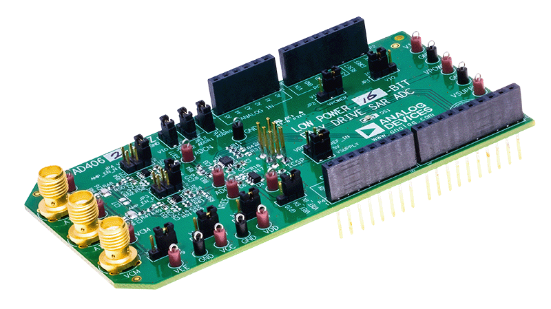
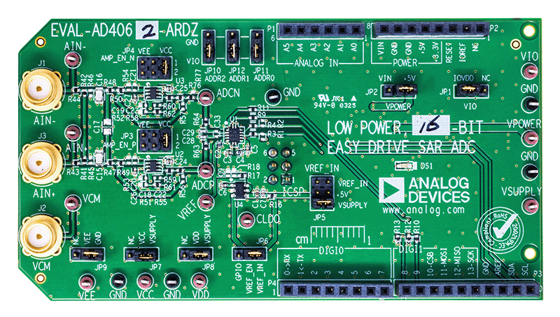

EVAL-AD4062
Evaluating the AD4060/AD4062 Compact, Low Power, 12-Bit/16-Bit, 2MSPS Easy Drive SAR ADCs
Resources
Latest Discussions
No discussions on AD4060 yet. Have something to say?
Start a Discussion on EngineerZone®