
Ultrasound Solutions
Medical ultrasound imaging modality uses high-frequency mechanical sound waves to view inside the body. Ultrasound imaging is a non-ionizing, real-time modality that allows clinicians to interrogate both the anatomy and physiology of body organs.
Ultrasound systems typically use high channel count electronics to transmit and receive ultrasound signals. Transmit circuitry typically generates high-voltage signals while receive circuitry typically detects high dynamic range low-voltage signals.
Analog Devices has a comprehensive portfolio of transmit, receive, power, and clocking components to support high-performance, compact, and low-cost ultrasound designs.
Value and Benefits
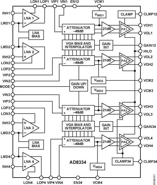
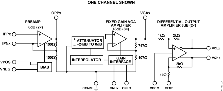
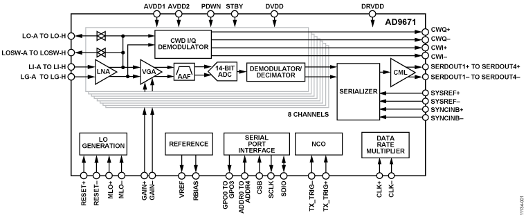
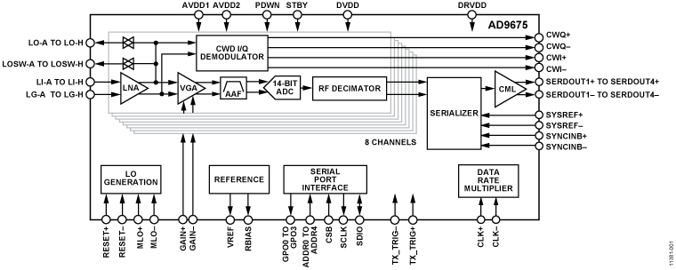
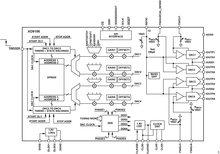
We offer a complete portfolio for ultrasound system circuitry. For transmit circuitry, we have high channel count, high voltage (HV) 3-level and 5-level pulsers that integrate transmit beamforming and transmit/receive switches. High-performance arbitrary waveform generator DAC and HV amplifier solutions are available for premium ultrasound systems. For the receive path, we offer high channel count, best-in-class analog front-end products. These AFEs include low noise amplifiers (LNAs), linear-in-dB variable gain amplifiers (VGAs), high dynamic range ADCs, per-channel digital processing, and LVDS or JESD interfaces. In addition to the Tx and Rx circuitry, we also have a large portfolio of best-in-class ultralow noise power management chips and ultralow jitter clocking solutions.


Features full complement of high-performance Tx, Rx, power, and clocking solutions
Guarantees high performance for classical ultrasound and advanced imaging modes
Provides highly integrated ultrasound transceivers for compact systems and digital probes
Featured Products
Interactive Signal Chains


Developer Tools and Resources
Design Tools

Simulation Models

Trainings and Tutorials


Files and Downloads
Book & eBook

Understanding Silent Switcher Technology: High Efficiency, Low EMI eBook
![]()
7.75 M
Circuit Note
CN0407: Ultrahigh Sensitivity Femtoampere Measurement Platform
![]()
548.59 K
CN0370: 16-Bit, Single-Supply LED Current Driver with Less than ±1 LSB Integral and Differential Nonlinearity
![]()
232.9 K
Data Sheet
ADGS1612: SPI Interface, 1 Ω RON, ±5 V, 12 V, 5 V, 3.3 V, Mux Configurable, Quad SPST Switch Data Sheet
![]()
373.21 K
Product Highlight
ADA4177 Family - Setting Industry Standards for Robustness
![]()
619.98 K
Product Selection Guide
Precision Products and Signal Chain Solutions: Selection Guide 2019
![]()
13.38 M
Tutorial
MT-230: Noise Considerations in High Speed Converter Signal Chains
![]()
255 kB
{{modalTitle}}
{{modalDescription}}
{{dropdownTitle}}
- {{defaultSelectedText}} {{#each projectNames}}
- {{name}} {{/each}} {{#if newProjectText}}
-
 {{newProjectText}}
{{/if}}
{{newProjectText}}
{{/if}}
{{newProjectTitle}}
{{projectNameErrorText}}