
安全性に関するアプリケーション・ノートの使用を通じた安全設計の支援 -パート3:機能安全性能の改善
シリーズの関連記事を読む
主なポイント
|
概要
機能安全(FS:Functional Safety)を実現するための回路について、故障モード影響診断分析(FMEDA:Failure Modes, Effects, and Diagnostic Analysis)の初回の反復を実施したとします。その場合に得られる結果は2つのうちいずれかしかありません。1つは、安全度水準(SIL:Safety Integrity Level)の要件を満たせたという結果です。もう1つは、要件を満たせなかったという結果です。では、要件を満たせなかった場合に、アーキテクチャを大幅に変更することなく対処するにはどうすればよいのでしょうか。そのためには、診断カバレッジ(DC:Diagnostic Coverage)の向上、動作条件の調整、安全性を高めるための対策の追加のうち、いずれかの手段を講じることになります。アナログ・デバイセズの安全性に関するアプリケーション・ノートには、そうした方法による設計の改善に役立つ情報が記載されています。それらを活用すれば、危険側故障の1時間当たりの平均確率(PFH:Probability of Dangerous Failure per Hour)、要求時の危険側故障の平均確率(PFDAVG:Probability of Failure on Demand Average)、安全側故障割合(SFF:Safe Failure Fraction)に対する要求を満たすことができます。本稿(本連載のパート3)では、FSに対応するコンポーネントに用意された安全性に関するアプリケーション・ノートを活用し、ICを含むシステムの機能安全性能を改善する方法について説明します。
FMEDAの例
本連載のパート2では、システムのFMEDAを実施する際、機能安全に関連するICの安全性に関するアプリケーション・ノートに記載された情報を活用する方法について説明しました。安全機能の設計が既にFSに適したアーキテクチャを採用している場合、初回のFMEDAによって良好な結果が得られる可能性があります。つまり、求められるPFH、PFDAVG、SFFを既に達成しているかもしれません。しかし、そうでない場合には設計の改善が必要になります。
一例として、表1にシステムのFMEDAの結果を示しました。具体的には、LDO(低ドロップアウト)レギュレータ「ADP7156」が、想定される1つのチャンネル(ハードウェア・フォルト・トレランス[HFT:Hardware Fault Tolerance]なし、つまりHFT = 0)の安全機能に及ぼす影響について評価しました。このFMEDAでは、以下の前提条件を設定しています。
- LDOレギュレータは、ロジック・コントローラに電力を供給します。
- LDOレギュレータの出力電圧が0Vである場合、安全機能は安全な状態になります。それ以外の場合、安全機能に影響を及ぼさないか、または安全機能の喪失につながる可能性があります。
診断については、過電圧(OV:Overvoltage)に関連する危険側故障に対して最大60%のDCが得られるように、安全遮断機能を備えるOV保護の手法(IEC 61508-2:2010の表A.9参照)を使用すると仮定します。また、安全機能は高頻度作動要求モード(High Demand Mode of Operation)で動作するものとします。更に、本稿で用いる故障率の予測はIEC 62380に基づいて実施すると仮定します。
| 名称 | コンポーネント | 機能 | 故障率 | 故障モード | FMD (%) | 影響 | 故障の分類 | DC (%) | λS (FIT) | λNE (FIT) | λDD (FIT) | λDU (FIT) |
| IC1 | LDOレギュレータ | イネーブルに設定した後、1.2ミリ秒以内に、3.3V±1.5%にレギュレートされた低ノイズの電圧を出力 | 7.15 FIT | VOUTがオフ、または0V付近でローの状態のままになる | 29 | 安全機能が安全な状態にある | 安全側 | — | 2.07 | |||
| VOUTが目標値より高い値にレギュレートされる | 12 | コントローラの損傷により安全機能を喪失 | 危険側 | 60 | 0.52 | 0.34 | ||||||
| VOUTが目標値より低い値にレギュレートされる | 9 | 安全機能の喪失 | 危険側 | 0 | 0.64 | |||||||
| VOUTがレギュレーションの範囲内で発振 | 6 | 安全機能に影響なし | 影響なし | — | 0.43 | |||||||
| VOUTがVIN付近の値のままになる | 24 | コントローラの損傷により安全機能を喪失 | 危険側 | 60 | 1.03 | 0.69 | ||||||
| VOUTのセトリング時間が1.2ミリ秒を超える | 3 | 安全機能に影響なし | 影響なし | — | 0.21 | |||||||
| VOUTがレギュレーションの範囲外で発振 | 1 | コントローラの損傷により安全機能を喪失 | 危険側 | 60 | 0.04 | 0.03 | ||||||
| システム機能への影響なし | 16 | 安全機能に影響なし | 影響なし | — | 1.14 | |||||||
| 0.39 FIT | VOUTがオフ、または0V付近でローの状態のままになる | 32.2 | 安全機能が安全な状態にある | 安全側 | — | 0.13 | ||||||
| VOUTが目標値より高い値にレギュレートされる | 6.8 | コントローラの損傷により安全機能を喪失 | 危険側 | 60 | 0.02 | 0.01 | ||||||
| VOUTが目標値より低い値にレギュレートされる | 6.8 | 安全機能の喪失 | 危険側 | 0 | 0.03 | |||||||
| VOUTがレギュレーションの範囲内で発振 | 3.4 | 安全機能に影響なし | 影響なし | — | 0.01 | |||||||
| VOUTがVIN付近の値のままになる | 20.5 | コントローラの損傷により安全機能を喪失 | 危険側 | 60 | 0.05 | 0.03 | ||||||
| システム機能への影響なし | 30.3 | 安全機能に影響なし | 影響なし | — | 0.12 | |||||||
| 小計 | 2.2 | 1.91 | 1.66 | 1.77 | ||||||||
* FMD( 故障モード分布: Failure Mode Distribution)
* DC( 診断カバレッジ: Diagnostic Coverage)
* FIT (故障率: Failure in Time)
SFFは、次式によって計算します1。
(1)
また、ICのPFHは以下に示す式によって算出することが可能です1。
(2)
上述した設計では、安全機能のSFFは69%で、PFHの寄与分は1.77FIT(故障率: Failure in Time)です。IEC 61508に基づいて、安全機能がSIL 2を達成する必要がある場合には、少なくとも90%のSFFが得られるようにシステムを設計しなければなりません。一方、SIL 2で許容されるPFHは100FIT~1000FITです。PFHの1%をICに割り当てると仮定すると、必要なPFHの寄与分は1FIT~10FITになります。下限値である1FITを目標にする場合、現在のアーキテクチャではSIL 2に必要なSFFとPFHの要件を満たせないことになります。
そこで、以下では、PFHとSFFを改善する方法について説明します。
DCの改善
式(2)を見ると、PFHは検出されない危険側故障率に正比例することがわかります。同様に、式(1)からは、SFFは安全側故障率と検出可能な危険側故障率が大きくなるほど高くなることが見てとれます。したがって、検出されない危険側故障率を低減し、検出される危険側故障率を高めれば、ICのPFHとSFFの両方が改善されます(図1)。
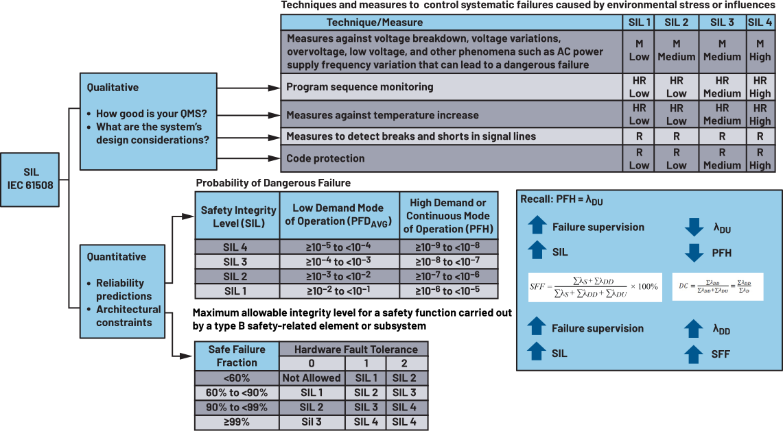
表1に示したFMEDAの例の場合、OVに関連する故障だけに対してDCが記載されています。ICの安全機能の性能を向上させる手段としては、DCの向上に関連する2つの方法が挙げられます。1つは、低電圧(UV:Undervoltage)に関連する危険側故障を検出するためのDCを導出することです。もう1つは、OVに関連する危険側故障のDCを向上させることです(例えば、60%から90%に引き上げる)。
上述した設計では、IEC 61508-2:2010の表A.9で規定された安全遮断という診断手法を用いるOV保護を採用しています。その場合、主張可能なDCの最大値は60%です。それに対し、ADP7156の出力を監視する2次側電圧監視という診断手法を採用すれば、主張可能なDCの最大値は99%になります。それらの診断手法を導入することにより、OVとUVの両方または規定の範囲外のあらゆる異常を監視できます。その結果、OV/UVに関連する危険側故障がカバーされます。これをFMEDAの例に適用すると、0.04FITのPFHと99.3%のSFFを達成できます(表2)。それにより、SIL 2の要求を上回る性能が得られます1、3。
信頼度予測の最適化
ICのPFHを改善するもう1つの方法は、推定故障率(FITの値)を下げることです。「安全性に関するアプリケーション・ノート」という連載記事のPart 1では、SN 29500で定められた方法、IEC 62380で定められた方法、アレニウスHTOLについて解説しました。ここで言うアレニウスHTOLとは、実験室での測定に基づいた高温動作寿命(HTOL:High Temperature Operating Life)のデータを使用し、アレニウスの式によって故障率を算出する方法のことです。同Part 1では、これらを使用してFSに対応するコンポーネントの故障率を計算する方法を示しました。安全性に関するアプリケーション・ノートに記載されている前提条件を用いることで、最も厳しい条件の値を使用するのではなく、提供された情報を活用して実際の動作条件に即した信頼度予測を実施することが可能になります。
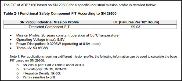
ここで、図2に示した例をご覧ください。これは、ADP7156の想定動作条件の下でSN 29500のFITに基づく信頼度予測を行った結果です。SN 29500に基づく信頼度予測は、電圧に依存する係数や温度に依存する係数といったアプリケーションに関連するパラメータの影響を受けます。そのため、想定したICの動作条件が実際のアプリケーションの条件よりも厳しいと考えられる場合には、実際の条件に合致するよう、動作電圧、動作周囲温度、ミッション・プロファイル、負荷条件などを調整できます。
| 名称 | コンポーネント | 機能 | 故障率 | 故障モード | FMD (%) | 影響 | 故障の分類 | DC (%) | λS (FIT) | λNE (FIT) | λDD (FIT) | λDU (FIT) |
| IC1 | LDOレギュレータ | イネーブルに設定した後、1.2ミリ秒以内に、3.3V±1.5%にレギュレートされた低ノイズの電圧を出力 | 7.15 FIT | VOUTがオフ、または0V付近でローの状態のままになる | 29 | 安全機能が安全な状態にある | 安全側 | — | 2.07 | |||
| VOUTが目標値より高い値にレギュレートされる | 12 | コントローラの損傷により安全機能を喪失 | 危険側 | 9 | 0.85 | 0.01 | ||||||
| VOUTが目標値より低い値にレギュレートされる | 9 | 安全機能の喪失 | 危険側 | 99 | 0.63 | 0.01 | ||||||
| VOUTがレギュレーションの範囲内で発振 | 6 | 安全機能に影響なし | 影響なし | — | 0.43 | |||||||
| VOUTがVIN付近の値のままになる | 24 | コントローラの損傷により安全機能を喪失 | 危険側 | 99 | 1.7 | 0.02 | ||||||
| VOUTのセトリング時間が1.2ミリ秒を超える | 3 | 安全機能に影響なし | 影響なし | — | 0.21 | |||||||
| VOUTがレギュレーションの範囲外で発振 | 1 | コントローラの損傷により安全機能を喪失 | 危険側 | 99 | 0.07 | 0.00 | ||||||
| システム機能への影響なし | 16 | 安全機能に影響なし | 影響なし | — | 1.14 | |||||||
| 0.39 FIT | VOUTがオフ、または0V付近でローの状態のままになる | 32.2 | 安全機能が安全な状態にある | 安全側 | — | 0.13 | ||||||
| VOUTが目標値より高い値にレギュレートされる | 6.8 | コントローラの損傷により安全機能を喪失 | 危険側 | 99 | 0.03 | 0.00 | ||||||
| VOUTが目標値より低い値にレギュレートされる | 6.8 | 安全機能の喪失 | 危険側 | 99 | 0.03 | 0.00 | ||||||
| VOUTがレギュレーションの範囲内で発振 | 3.4 | 安全機能に影響なし | 影響なし | — | 0.01 | |||||||
| VOUTがVIN付近の値のままになる | 20.5 | コントローラの損傷により安全機能を喪失 | 危険側 | 99 | 0.08 | 0.00 | ||||||
| システム機能への影響なし | 30.3 | 安全機能に影響なし | 影響なし | — | 0.12 | |||||||
| 小計 | 2.2 | 1.91 | 3.39 | 0.04 | ||||||||
* FMD( 故障モード分布: Failure Mode Distribution)
* DC( 診断カバレッジ: Diagnostic Coverage)
* FIT (故障率: Failure in Time)
安全性を高めるための追加の対策
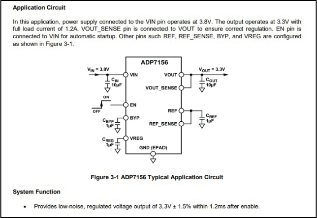
安全性に関するアプリケーション・ノートには、解析の対象として想定される回路例が掲載されています(図3)。また、同アプリケーション・ノートの故障モード分布(FMD:Failure ModeDistribution)のセクションには、システムの故障モードについての記載があります。それらを利用し、必要に応じて安全性を高めるための対策を追加することで、各故障モードに対処する方法を決定できます。例えば、出力のOVに関連する危険側故障に対しては、ツェナー・ダイオードやヒューズなどの保護手段を追加することで対処することが可能です。つまり、この方法を適用すれば、ツェナー・ダイオードによってOVをクランプすることができます。このようにして故障の影響が生じないようにすることで、危険側故障が排除されます。その結果、PFHとSFFを改善することが可能になります。
まとめ
厳格なSILの要件を達成するためには、必ずしもシステムのアーキテクチャを全面的に見直す必要はありません。多くの場合、的を絞った診断データや信頼性データを活用することにより、既存の設計を戦略的に改良することが求められます。アナログ・デバイセズが提供する安全性に関するアプリケーション・ノートは、様々な知見を提供しています。それらを活用することで、DCの強化、動作条件の最適化による推定故障率の低減、外付けの保護用回路などを用いた補助的な対策を実現できます。結果として、機能安全性能(具体的には、SFFとPFH/PFDAVG)を体系的に向上させることが可能になります。本稿では、LDOレギュレータ(ADP7156)を具体的な例にとりました。その例からわかるように、基本的なOVの遮断から2次側の電圧監視への移行を図ることで、SIL 2の要求を満たせない状態から、それを上回るレベルまでの劇的な改善が得られます。安全性に関するアプリケーション・ノートは、安全性を確保するための設計を支援する重要なロードマップとして機能します。また、同アプリケーション・ノートを活用すれば、使用するICが、IEC 61508の厳しい要件を正確かつ効率的に満たすようにすることが可能になります。
References
1Bryan Angelo Borres「安全性に関するアプリケーション・ノート 【Part 2】故障モード分布」Analog Dialogue、Vol. 59、2025年10月
2Bryan Angelo Borres「高性能の電圧監視ICにより、産業分野向け機能安全規格への準拠度を高める 【Part 2】SILのレーティングに対応するコンポーネントの活用」Analog Devices、2025年3月
3Bryan Angelo Borres and Noel Tenorio「産業向け機能安全に対応する電源の設計 【Part 1】IEC 61508が教えてくれること」Analog Devices、2025年7月