How to Drive the LTC2387 (Part 1): Signal Applications to 5MHz that Require Low Inter-Modulation Distortion
How to Drive the LTC2387 (Part 1): Signal Applications to 5MHz that Require Low Inter-Modulation Distortion
2016年05月13日
The biggest challenge in driving a 15Msps, 18-bit ADC with an 8Vp-p input range is the lack of integrated amplifiers with adequate bandwidth, low noise, and the required output excursion. There are low-noise, high-BW amplifiers than can produce 2VPP. There are low speed amplifiers than can produce 8VPP. For low distortion beyond 1MHz, a composite amplifier involving a mix of devices built with different processes, and operating on different supplies appears to be the only viable option.
The use of discrete transistors in a composite amplifier is not popular with customers, nor is it necessarily easy to produce extremely high linearity in a discrete implementation. The physical space required of a complex discrete transistor based feedback amplifier, or even a composite amplifier involving even a limited number of discrete transistors, results in excessive delay in the physical propagation paths, thereby creating a potential loop stability problem.
The following will detail a composite amplifier involving only integrated amplifiers. In this case, although as compact as possible, physical path length can still be an issue. As such, certain circuit features are incorporated to address what could be considered layout issues. See Figure 1.

Figure 1. Two Tone Experiment Driving the LTC2387
Unfortunately, a high linearity amplifier, even intended for modest bandwidth, requires a high GBWP in order to have an adequate feedback factor. The lower the required distortion, the more GBWP is needed to produce that distortion level at a given frequency. This means there will be a great noise BW that must be suppressed after the final stage amplifier and before the ADC. There are topologies that may have low noise density at low frequency, and depend on digital filtering to reduce the noise contribution of the those portions of the first and second Nyquist zone that fall near the Nyquist boundary, however, the driver must adequately suppress noise before the first alias bands fold into the band of interest. That great GBWP, and the resulting noise BW, the double-edged sword in a high linearity amplifier, would be limited to some extent by the ADC itself. However, in the case of this ADC the full 200MHz input BW would fold 26 times into the 7.5MHz baseband. The noise density of the ADC, in the 7.5MHz Nyquist BW, would be 16nV/√Hz. But a driver, without BW limiting, would require an output noise density of about 3nV/√Hz in order to be comparable in noise contribution to the ADC itself. Clearly, 3nV/√Hz output referred is not possible at 8Vpp and gain in the 6-12dB range. Even practical 400ohm FB resistors in a differential amplifier have noise contribution that is greater than this. As the amplifier must drive these feedback resistors, becoming part of the load, using lower impedance is not an option. Lower impedance will increase the distortion in the output stage, defeating the purpose. Lower impedance in the feedback, would also require a low, and very constant source impedance feeding the input of the differential amplifier, or it would also result in distortion. Many sources, buffers, amplifiers, sensors, or even some passive filters may not have constant output impedance, and will produce distortion if loaded with low impedance. The input amplifier noise gain, noise voltage, and noise current, all conspire to elevate output noise density.

Figure 2. Prototype Populated with LT6237, LTC6404, and LT1396 (Postage stamp 34mm × 24mm)
This need to limit noise bandwidth demands an output filter, placed post amplifier. That filter must settle very quickly, and yet suppress even the first alias bands around the clock frequency, as well as the extended bandwidth that results from the high GBWP.
Most integrated amplifiers intended to drive high speed ADCs have limited supply ranges, and are often characterized at 2VPP. They often have little margin above this signal level. The core of this composite amplifier does contain a low voltage high bandwidth differential amplifier, but it will require an output stage capable of delivering 8VPP, with enough margin to accommodate the insertion loss of a filter, as well as the complex impedance of that filter.
The following is then a description of a composite amplifier involving input buffers of several types followed by a composite differential amplifier based on the LTC6404 followed by fixed gain output stages using current feedback amplifiers.
The LT1396 dual 400 MHz CFA, in MS8, as the output stage is not the only candidate, or even the best candidate, but was chosen for the PCB implementation in order to have the option of several alternatives. Note that practical current feedback amplifiers do not have rail-rail output stages. The reason for having a current feedback amplifier as the output stage is the combination of fast settling, low delay, high slew, and low output impedance at high frequency. Extremely low distortion and low noise in the output stage would be nice, but is not imperative. High slew rate, and low delay are more important.
The LT1396 is only practical as a driver for this application because it is within a control loop established by the LTC6404, and within the control loop bandwidth, its noise and distortion contribution is reduced. Without this correction for its errors, the LT1396 would seriously compromise both SFDR and SNR.
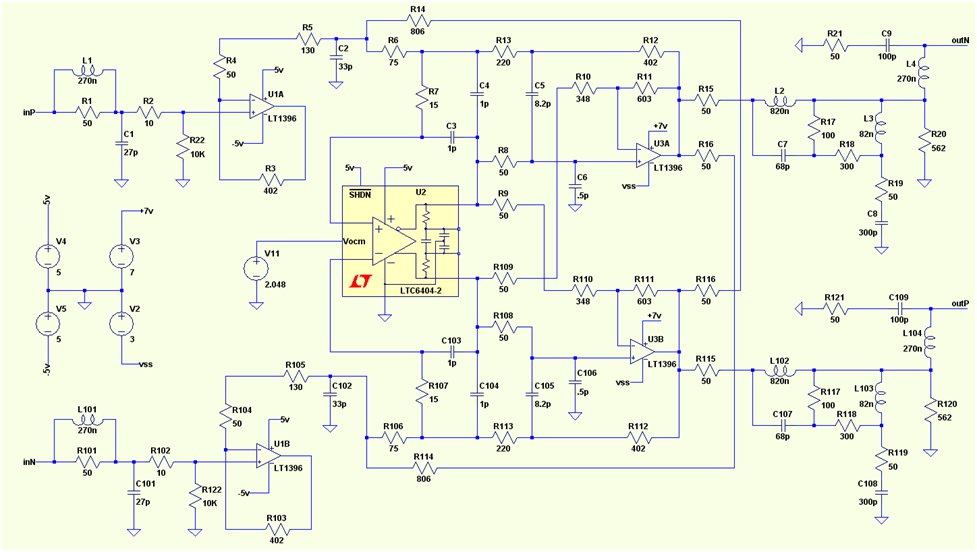
Figure 3. Amplifier Topology
There is a cross-over feature in the feedback path that places high frequency feedback around the differential amplifier (U2), and global feedback around the entire loop. The global feedback is in fact rolled off at about 100MHz by the same element that produces a high pass for the local compensation (C5). At 1MHz, the feedback current local to the differential amplifier is approximately 60dB below the global current feedback. The output amplifier (see U3 in Figure 2) is then limited by its own performance approaching this cross-over region, and would produce unacceptably high noise density and distortion products above a certain frequency. These products however are suppressed by an output filter that also suppresses the first aliased noise bands by some 10dB, and 2nd alias bands by 15dB. The attenuation increases beyond this point, but not dramatically so. This post filter is absorptive in order to minimize interaction, and obtain the highest SFDR possible from the ADC.
The overall loop gain is a product of both positive and negative feedback. The positive feedback (R14) exhibits an extended path length, and delivers it to a shunt capacitor (C2) prior to the differential amplifier (U2). The positive feedback raises the load impedance seen by the input buffers (U1), provides some compensation for lag in the negative feedback path, and allows higher gain with comparatively low source impedance seen by the differential amplifier. It also acts as an active filter, in that it increases the gain in the pass-band, but in the stop band, there is little remaining positive feedback, dominated by the negative feedback. The combination of positive and negative feedback also raises the common mode input voltage seen by the differential amplifier when driven from ground referenced signals. Baring the use of positive feedback in this fashion, a pull-up may be required.
The combination of positive and negative feedback also extends the common mode range of the amplifier as a whole by limiting the common mode seen by the differential amplifier. In doing so, although it raises the differential impedance seen by the input buffers, it reduces the common mode impedance.
The input stages (see Figure 3) are also current feedback amplifiers, configured in a fashion where the input stage is used as though they are 4 transistor complementary emitter followers, the output taken from the inverting input. The loop is closed around these amplifiers, by the recommended minimum 400 ohms (R3), but the actual output is not used. The PCB however has provision for taking output from the output terminal in case other amplifiers are used.
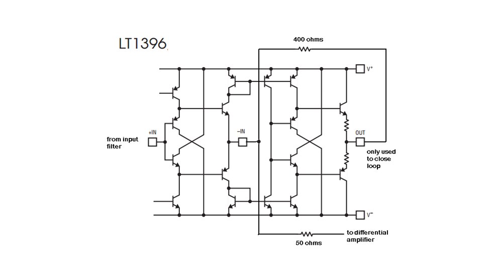
Figure 4. Simplified internal schematic of LT1396
The LT1396 output stages however, are used as conventional current feedback amplifiers, with a gain of approximately 2. The output stage has both inverting and non-inverting gain.
AV = 0.5+ (603 / (348+49.9) = 2.015
The output amplifiers are each driven by both outputs of the differential amplifier: each output of the LTC6404 driving the non-inverting input of one amplifier, and the inverting input of the other amplifier. In order to reach 8.192VPP full scale, the LTC6404 must deliver 2.0VPP.
The non-inverting path has compensation elements, and the non-inverting path is unavoidably delayed by a more circuitous path, involving buried traces and a cross-over. The positive feedback path is similarly more circuitous as it also must cross over. The positive feedback path can be extended to some extent without compromising stability. The negative feedback path should not be extended.
Although the LTC6404 has local zero-compensation for input and pad capacitance, the dominant compensation element is C5, and its counterpart in C105. (add 100 for the counterparts) This capacitor intercepts the global (DC) feedback path, and is a zero for the differential amplifier; however, it is a pole for the output amplifiers. The main negative feedback resistor R12, is also the most serious load for the output amplifier. This resistor is physically large to potentially improve distortion. Understanding this topology requires recognition that C5 can potentially conduct positive feedback back into the output stage. The point at which C5 intercepts the negative feedback must not be capable of producing in the source termination resistor R8, enough signal to significantly raise the output impedance of U2, or indeed, in the extreme produce sustained oscillation. The value of R12, should be greater than the sum of values between C2 and C5, and is related to the noise gain in the output stages. Capacitor C2 is also instrumental in assuring that the noise gain of the differential amplifier is high enough to ensure stability with the type of LTC6404 that is chosen.
The LTC6404-1 is best suited for lower gain implementations, but the LTC6404-2, or even the -4 version can be used for higher gain or higher frequency versions, with the appropriate choice of R13/R6. There are numerous 50 ohms resistors throughout the design, and these are to ensure that the longer transmission lines in the various signal paths, forward or reverse, are either correctly source terminated or end terminated. As the transients delivered by the ADC have quite high frequency content, and as, at 15Msps, this amplifier only has 29 nsec to settle to 18-bit levels, control of VSWR is important.
The Input Filter
The input filter on the PCB as implemented is designed to provide as low a source impedance as possible in band, for good noise figure, but also to provide a well damped and RFI filtered port. The ceramic core inductor (L1) looks like a short at low frequency, but 50 ohms at high frequencies, due to R1. Do not be tempted to replace this parallel combination of inductor and resistor with a ferrite bead. Beads will cause distortion. There is a 10K input resistor (R22) to ground, to act as a bias source, in case a DC blocked signal source is applied. This resistor can be removed if the signal source provides DC bias within an acceptable common mode input range. The resistor can be lower if necessary, or it can be higher within reason. If a higher input impedance is desired, it should be noted that the LT1396 may exhibit up to 30uA input bias current, and 6pA noise current. For very low bias current high source impedance, applications, the LTC6269 can be used, although the noise level is higher, and the usable frequency range may be more restricted.
For lower frequency applications where noise figure is important, the 1.1 nV/√Hz LT6237 can be used, including providing some differential gain before the LTC6404. The input noise figure of 1.1 nV/√Hz, in 7.5 MHz BW, suggests that this could be followed by up to about 24dB gain before it dominates the ADC. In fact, other noise sources, or impedances throughout the signal chain impose a practical limit of about 20 dB. Beyond that point, the modest improvement in noise figure is at the expense of dynamic range. In the 20dB case, the LTC6404 controlled driver section should arguably have a gain between 6 and 12 dB gain. The driver stage gain should be 6dB for the best noise figure, 12dB for the lowest distortion. This means the input stage would be configured, respectively, for between 14dB, and 8dB. Even at 14dB gain, the impedance seen at the inverting inputs of the first stage will limit the noise figure that can be achieved. Conventional wisdom would suggest that the gain in the input stage be maximized, to minimize the impedance at the gain setting resistors, but this means, a low value feedback resistor as well (at about 4X the gain setting resistor), and as a result, likely to increase distortion. The signal swing that can be developed by the input stage will, in all likelihood, be limited to some 2Vpp, although, for lower frequency applications, it may be practical with as much as 4Vpp. Of course, if the best noise figure is required, at the expense of dynamic range, the gain in the input stage can be raised considerably. The PCB is not designed for gain setting resistors of less than 50 ohms (not shown on Figure 2) , as there are transmission lines between these resistors on the PCB. But FB resistors (R3) of 500 ohms or more could be considered.
The Output Filter
Much like any direct sampling ADC, the LTC2387 produces mixing products, seen as glitches, which must not reflect and return to the ADC at the wrong time—the wrong time meaning when sampling. They must also not elicit ringing from the filter, or any of the amplifiers. Ringing may preserve remnants of non-linear charge, and thereby cause distortion. These transients must also not result in output voltage or current dependent recovery artifacts from the amplifiers, as these are likely to be non-linear in nature even if the transients themselves were not.

Figure 5. Output Filter Characteristics
Completely absorptive filters will necessarily settle very well. If there is no return reflection, there will be nothing to settle out. However, a completely absorptive filter is not easy to achieve. Additionally, many absorptive filters with modest stop-band attenuation, may allow transients returning to the amplifiers to disturb them. In this case, amplifier recovery will be an issue if not fast, and consistent with output excursion.
Many amplifiers will exhibit variation in output impedance with output current or voltage, producing variability in the disturbance allowed into earlier input stages. Maintaining a high degree of absorption, and a high degree of isolation, can be conflicting requirements. The transients could disturb the output amplifiers, themselves. They can potentially reflect all the way through the chain, much like in an RF amplifier with poor reverse isolation, to disturb the input buffers, or even prior to the input buffers. The use of rail to rail output amplifiers, either in the output stage or the input buffers, will render the results more sensitive to the reflectivity of the original signal source. As the output impedance of amplifiers rises with frequency, and as the MS8 package is not the best choice, this is in fact an issue. Similar population of a version with the output amplifier in a DFN produced 15dB improvement in IM results over the MS8 in a test where the output filter is replaced by simple 50 ohm source termination. However, with the output filter intact, it is more difficult to gauge the difference.
The transient that develops in the output impedance of the final amplifiers will be non-linear, and if allowed to propagate back through the feedback network into the LTC6404 input stage, is less likely to settle within the available time, due to the overcompensation of the differential amplifier.
The filter shares features with elliptical filters and diplexers. It appears very absorptive below 5MHz, and has better than 20dB return loss up to about 1GHz. This frequency range matters as there are transients delivered by the ADC that extend to these frequencies. These are 50 ohm source terminated filters.
The output filter has implications beyond the trade-off of complexity vs desired response. A greater degree of over-compensation of the differential amplifier will push up the noise gain of the output stage at a lower frequency, requiring a lower corner frequency in the output filter. It also reduces the control bandwidth exerted on the LT1396 output stage, resulting in ineffective suppression of spurs related to crossover distortion. The output filter response is dictated to a large extent by the spectral noise distribution from the amplifier topology, and by the need to suppress alias noise bands around fs and beyond. It is not a true anti-aliasing filter, and in fact, would not be adequate as an anti-aliasing filter if the input spectral power distribution were flat. This type of response, in this location, would often be referred to as a roofing filter. The choice of sample rate has a large bearing on the desired stop band, but is limited by the physical size, and SRF of inductors. In fact, the SRF of the final inductor can be a major impediment in maintaining adequate absorption to GHz frequencies. This ADC has such high SNR that aliased noise is likely to render many potential driver solutions unworkable. The filter shown above suppresses the 1st two alias bands by about 10dB, and the second two alias bands (30MHz) are suppressed by 15dB. This would result in an elevation of the noise density below 1 MHz by about 1 dB, relative to baseband alone. Including the alias bands around 45MHz, and 60MHz, raises the noise floor by a further 0.25dB.

Figure 6. Two Tone Test at 485 and 519 KHz. (note IM3) (ignore SNR/floor)
For many natural phenomena, like vibration, spectral power distribution falls off by 12-18 dB per octave. If full power were expected at 200 KHz, thereafter rolling off by 18dB per octave, the filter as shown would be adequate for anti-aliasing purposes. 7 octaves*18dB, + 10dB suppression around 15MHz would reduce the first expected aliasing to essentially –118dB, arguably removing it from consideration.
Sensing applications involving excitation frequencies extending out to several MHz are practical as the spectral power distribution is limited, and under control.
Performance
There have been quite a number of variants constructed, and scenarios tested, but presentation of the volume of data, and schematics, as well as strengths and weakness of the variations is beyond the scope of this article.
These figures are summary.
Plots for specific scenarios can be provided upon request.
SNR 89dB with 12dB gain (shown Figure 2 & 5) to 91.9dB with gain of 6dB (schematic on request)
IM3 at 500 KHz(–7dBfs / tone) –115dBfs at 10Msps, (–113dBfs at 15Msps)
IM3 at 1MHz –110dBfs at 15Msps at gain = 12dB, –115dBfs at gain = 6dB (LT1396 at U1 and U3)
IM3 products at 3MHz are approximately 100dBfs
SNR includes ADC contribution. Best performance is with no input capacitors at the ADC, using ADC demo board.
In Figure 5, the spectrum was masked to produce the correct calculation of IM3 products by having the average noise floor, as elevated by generators, similar to the point where the IM3 products appear.
Variants
This driver board can be built in a large number of alternative populations depending on bandwidth, or rather, spectral power distribution; gain; input impedance and power constraints.
There are population options that have not been tested to great extent, and optimization of the output filter may produce improved results as there is evidence that performance is limited by interaction with the filter, and with the transmission lines on the prototype boards. If this driver were implemented on the same board at the ADC, transmission lines can be much shorter, lower impedance, and without certain features on the demo board that may be limiting performance.
The choice of output amplifier may be limited if the filter were redesigned for significantly less than 50 ohms. There is evidence that lower impedance, or more highly absorptive drive is beneficial, possibly producing IM3 of –125dBfs at 1 MHz. (Part III of this series)
For those applications that need low power, U1 can be the LT6203, with U2 as the LTC6406, or even LTC6403. This would be limited to 100kHz full power, although for vibration analysis with dramatic roll-off with frequency, it may be fine with content to several MHz. The LTC6403 has higher noise voltage than the LTC6406, and, as a result, it would be better suited to lower gain versions.
For low input impedance applications, the input buffer can be bypassed (removed) and SNR and even linearity may be better. Tests of this aspect have revealed that IM can be worse, as can distortion, if the source of the signal does not have constant and fairly low output impedance, including extending to high frequency.
The LT6237 will produce better SNR than the LT1395 as the input buffers, but SFDR will degrade beyond 300-500 KHz .
The LT6237, and likely other RRIO amplifiers, are more adversely affected by reflections from prior filters, and have reduced high frequency reverse isolation compared to the current feedback amplifiers. Other current feedback amplifiers available in MS8 can be used and have been tested on this PCB. Only current feedback amplifiers should be considered for the output stage.
For very high input impedance applications, the LTC6269IMS8 can be used, but it is limited to ±2.5V supplies, so only fairly high gain is practical, and as a result, SNR will suffer. Usable bandwidth may extend to 5MHz, however.
With changes to the artwork, other amplifiers could be used. The LT6411 is likely to perform better than the LT1395 as the output stage, but no pin-compatible alternatives would be available. The LTC6409 could be used as an alternative to the LTC6404, but it has higher noise current, and may only make sense for higher gain versions. The use of a single input buffer would simplify the artwork, as well as improve SNR. The design as is can be used for single ended or differential signals. The common mode range is limited to +2V, and –1V relative to ground in higher gain versions. With lower gain, common range can be extended, depending on input buffers and power supplies. Common mode range can possibly be extended considerably if SNR can be surrendered. The addition of a common mode servo prior to the LTC6404 can greatly extend common mode range.
Applications
Most practical applications for this driver will be receiving those signals that result from relatively high levels of excitation, and similarly may produce relatively high output. Doppler flow measurements, ultrasonic measurements that cannot use time-gain amplifiers, and medical imaging, may be examples. Vibration analysis is one area that may benefit, although it would be expected that MHz frequencies would exhibit very low power levels. The use of pre-emphasis, or differentiation may allow the performance to several MHz to be of considerable benefit. Sonar, hydrophones and geophones can also produce considerable signal power, and the frequency range and dynamic range are likely interesting to those fields. The use of spread spectrum modulation for long distance sonar would be sensitive to inter-modulation distortion between colliding reflections from different returns, and so, would presumably benefit from this driver and ADC. The use of excitation signals out to several MHz in EM sensing, eddy current sensing, metal detection or characterization of materials, would be expected to be of interest. The use of this topology to receive output from a trans-impedance amplifier (TIA) intended for high optical power levels may be of interest. The use of this driver as a means of aggregating multiple signals, or as a combiner, possibly with many inputs, for low frequency multi-tone signals can also be considered, assuming it is to be used to drive the LTC2387... of course.


