AN-1510: Precision, Bipolar Configuration for the AD5450/AD5451/AD5452/AD5453 8-Bit, 10-Bit, 12-Bit, and 14-Bit Multiplying DACs
Circuit Function and Benefits
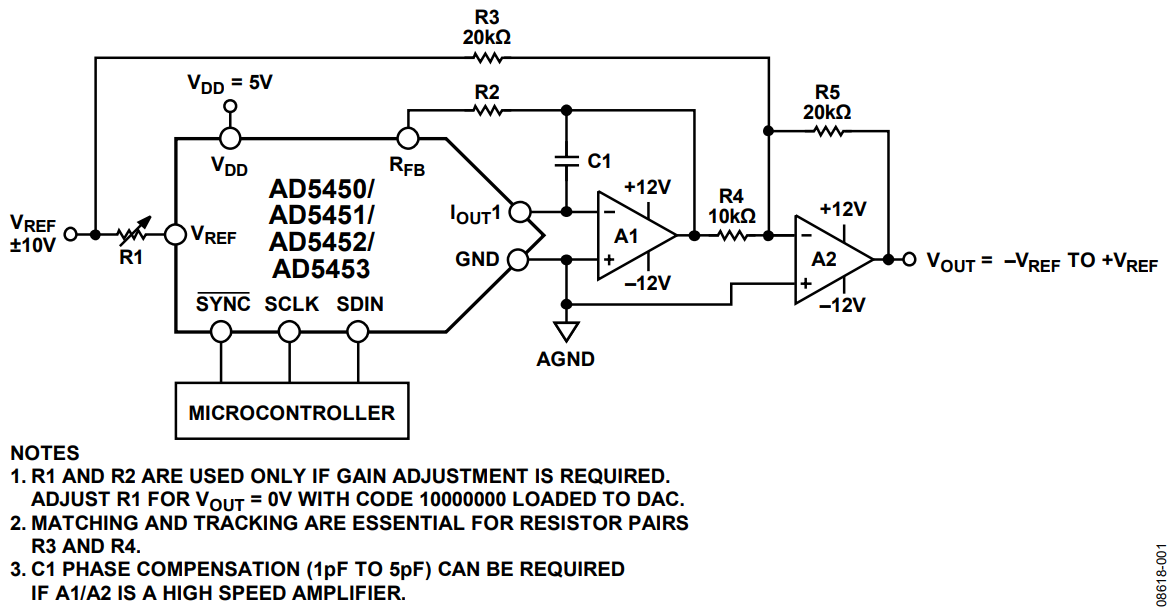
The circuit shown in Figure 1 is a precision, bipolar, digital-to-analog (DAC) configuration that uses the AD5450/AD5451/ AD5452/AD5453 precision multiplying DAC and the AD8066 low noise operational amplifier (op amp). The DAC is the core programmable element, and the amplifier selection dictates the performance in terms of precision or speed. For an accurate, high precision, low noise application, the AD8066 dual op amp can be used to provide the current to voltage (I to V) conversion and signal conditioning. A low noise reference such as the ADR01 is required to drive the reference voltage (VREF) input, and optimum output noise performance is obtained by using a low noise, low bandwidth output amplifier. The main advantages of this circuit are simplicity, constant reference input impedance, and the ability of the VREF reference voltage to exceed the DAC supply voltage (VDD).

Circuit Description
In many applications, it can be necessary to generate a full, four quadrant multiplying operation, or a bipolar output voltage swing, as shown in Figure 1. This can be accomplished by using a dual amplifier, indicated by the A1 and A2 amplifiers, and the R2, R3, R4, and R5 external resistors. In this circuit, the A1 amplifier performs the I to V conversion, and the second amplifier, A2, provides a gain of 2. Biasing the external amplifier with an offset from the reference voltage results in a full, four-quadrant multiplying operation. The ADR01 is a suitable reference to drive the reference inputs in dc applications. The ADR01 is a high accuracy, high stability, 10 V precision voltage reference. Because the ADR01 temperature coefficient (TC) and long-term drift are primary considerations for applications requiring high precision conversion, this device is an ideal candidate.
The AD5450, AD5451, AD5452, and AD5453 DACs are designed on a 5 V complementary metal-oxide semiconductor (CMOS) process and operate from a VDD power supply of 2.5 V to 5.5 V. These DACs accept VREF input ranges of up to ±10 V as shown in Figure 1, and the power supply for the output amplifiers must be a bipolar supply with enough headroom to accommodate the analog voltage output range, VOUT. The transfer function of this circuit shows that both negative and positive output voltages are created as the input code, D, is incremented from Code 0 (VOUT = −VREF), to midscale (VOUT = 0 V), to full-scale (VOUT = +VREF).
Calculate the value of VOUT with the following equation:
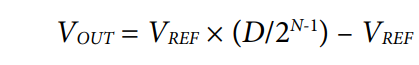
where:
N is the resolution of the DAC.
D is the digital word loaded to the DAC, and D = 0 to 255 (8-bit
AD5450), D = 0 to 1023 (10-bit AD5451), D = 0 to 4095 (12-bit
AD5452), or D = 0 to 16,383 (14-bit AD5453).
An op amp is used in the I to V conversion stage of this circuit. The supply voltage of the op amp limits the reference voltage that can be used with the DAC. The input bias current and input offset voltage of an op amp are important selection criteria for precision current output DACs. This circuit uses the AD8066 op amp, which has an ultralow input offset voltage (0.4 mV typical) and input bias current (2 pA typical).
The input offset voltage of an op amp is multiplied by the variable noise gain (due to the code dependent output resistance of the DAC) of the circuit. A change in this noise gain between two adjacent codes produces a step change in the output voltage due to the input offset voltage of the amplifier. This output voltage change is superimposed on the desired change in output between the two codes and produces a differential linearity error, which, if large enough, can cause the DAC to be nonmonotonic.
In general, the input offset voltage should be a fraction of an LSB to ensure monotonic behavior when stepping through codes. The compensation capacitor, C1, prevents ringing or instability in the closed loop. Typical values in the 1 pF to 5 pF range can be used.
Careful consideration of the power supply and ground return layout ensures the rated performance of the circuit. When designing the printed circuit board (PCB), separate and confine the analog and digital sections to certain areas of the board. If the DAC is used in a system where multiple devices require an AGND-to-DGND connection, make the connection at one point only. Establish the star ground point as close as possible to the device.
These DACs must have ample supply bypassing of 10 μF in parallel with 0.1 μF on the supply located as close to the package as possible, ideally right up against the device. The 0.1 μF capacitor must have low effective series resistance (ESR) and low effective series inductance (ESL), similar to the common ceramic types that provide a low impedance path to ground at high frequencies, to handle transient currents due to internal logic switching.
Apply low ESR, 1 μF to 10 μF tantalum capacitors at the supplies to minimize transient disturbance and filter out low frequency ripple. To optimize high frequency performance, place the I to V amplifier as close to the DAC as possible.
Common Variations
The OP2177 is an ideal dual op amp candidate for the I to V conversion circuit. It also provides a low input offset voltage (15 µV typical) and ultralow input bias current (0.5 nA typical). The ADR02 and ADR03 with 5.0 V and 2.5 V (typical) output, respectively, are other low noise references available from the same reference family as the ADR01. Other suitable low noise references are the ADR441 and ADR445. The size of the reference input voltage is restricted by the rail-to-rail output voltage of the selected op amp.
参考資料
ADIsimPower™ Voltage Regulator Design Tool.
Kester, Walt. Chapter 3 and Chapter 7. The Data Conversion Handbook. Analog Devices. 2005.
MT-015 Tutorial. Basic DAC Architectures II: Binary DACs. Analog Devices.
MT-033 Tutorial. Voltage Feedback Op Amp Gain and Bandwidth. Analog Devices.
MT-035 Tutorial. Op Amp Inputs, Outputs, Single-Supply, and Rail-to-Rail Issues. Analog Devices.
MT-101 Tutorial. Decoupling Techniques. Analog Devices. Voltage Reference Selection Wizard