AD4062
新規設計に推奨Compact, Low Power, 16-Bit, Easy Drive SAR ADC with I3C Interface
- 製品モデル
- 3
- 1Ku当たりの価格
- 最低価格:$8.90
製品情報
- Small footprint, big performance
- INL: ±0.5 LSB maximum
- SNR: 86.1dB with VREF = 3.3V
- 1.35nJ per conversion
- 405μW at 300kSPS in sample mode
- 370μW/112μW at 1MSPS/300kSPS in autonomous modes
- 4.1μW standby power
- Versatile signal conditioning integration
- Easy Drive features enable small, low-power AFE designs
- Compatible with differential and single-ended signal chains
- Wide common-mode input range
- Minimizes digital host activity and power dissipation
- Autonomous sampling with window comparator and interrupt generation
- Averaging filter with burst sampling support
- Power cycling synchronization for companion devices
- 2-wire I3C Interface compatible with 1.8V to 3.3V logic
- 2.00mm × 2.6mm LFCSP and 1.67mm × 1.97mm WLCSP
- Wide operating temperature range: −40°C to +125°C
The AD4062 is a versatile, 16-bit, successive approximation register (SAR) analog-to-digital converter (ADC) that enables low-power, high-density data acquisition solutions without sacrificing precision. This ADC offers a unique balance of performance and power efficiency, plus innovative features for seamlessly switching between high-resolution and low-power modes tailored to the immediate needs of the system. The AD4062 is ideal for battery-powered, compact data acquisition and edge sensing applications.
The Easy Drive features enable highly efficient analog front end (AFE) designs. The small sampling capacitors (3.4pF) maximize input impedance, thus reducing the dependence on high-bandwidth, power-hungry amplifiers typically required by SAR ADCs. The wide input common-mode range grants inherent support for both differential and single-ended signals.
The AD4062 supports microcontrollers with power-down modes and interrupt-driven firmware. The autonomous modes enable out-of-range event detection while the digital host sleeps. The burst averaging mode delivers on-demand, high-resolution measurements while offloading computations from the host processor. The self-timed device enable signal (DEV_EN) synchronizes AFE device power cycling to the ADC sampling instant, optimizing system power consumption while minimizing power-up settling error artifacts. The AD4062 also supports power cycling the voltage reference and using the supply as the ADC reference voltage (VREF) for additional power savings.
The device configuration and ADC data readback is supported via a robust, 2-wire I3C interface with cyclic redundancy check (CRC) supported for all data transfers. The AD4062 is available in compact 14-Lead Lead Frame Chip Scale [LFCSP] and 16-Ball Wafer Level Chip Scale [WLCSP] packages and operates across a wide temperature range, making it ideal for a diverse set of applications.
APPLICATIONS
- Battery-powered data acquisition
- Vital signs monitoring
- Biological and chemical analysis
- Geologic and seismic sensing
- Motion and robotics
ドキュメント
データシート 1
ユーザ・ガイド 1
デバイス・ドライバ 1
| 製品モデル | ピン/パッケージ図 | 資料 | CADシンボル、フットプリント、および3Dモデル |
|---|---|---|---|
| AD4062BCBZ-RL7 | WLCSP | ||
| AD4062BCPZ-R2 | LFCSP | ||
| AD4062BCPZ-RL7 | LFCSP |
これは最新改訂バージョンのデータシートです。
ソフトウェア・リソース
デバイス・ドライバ 1
評価用ソフトウェア 1
必要なソフトウェア/ドライバが見つかりませんか?
ハードウェア・エコシステム
ツールおよびシミュレーション
LTspice
下記製品はLTspiceで使用することが出来ます。:
- AD4062
Signal Chain Designer
Signal Chain Designerは、複雑な高精度シグナル・チェーンの構築、シミュレーションを行うために設計されたウェブベースのツールです。PCBを作成する前に、伝達関数、ノイズ、消費電力、入力範囲、DCエラーなど、回路の性能を確認できます。さまざまな部品やアーキテクチャを素早く試すことができます。シグナル・チェーンはLTspiceにエクスポートして更に解析を行うことができます。
ツールを開く
LTspice®は、無料で提供される強力で高速な回路シミュレータと回路図入力、波形ビューワに改善を加え、アナログ回路のシミュレーションを容易にするためのモデルを搭載しています。
評価用キット
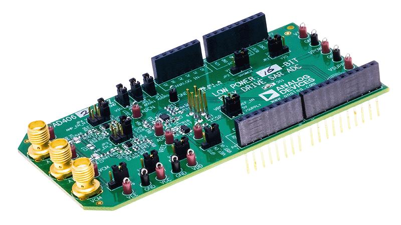
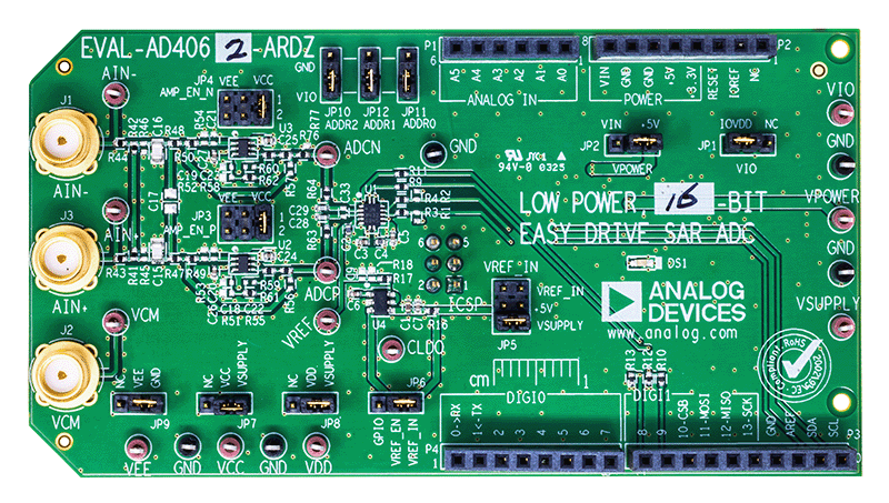
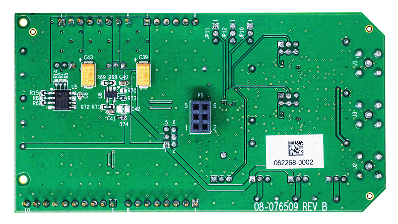
EVAL-AD4062
AD4060/AD4062(コンパクト、低消費電力、12ビット/16ビット、2MSPS Easy Drive SAR ADC)の性能評価
資料
最新のディスカッション
AD4062に関するディスカッションはまだありません。意見を投稿しますか?
EngineerZone®でディスカッションを始める