Optimizing LDO Headroom Control with a Current Reference Switching Regulator Design—Part 2: Design, Implementation, and Evaluation Results
Optimizing LDO Headroom Control with a Current Reference Switching Regulator Design—Part 2: Design, Implementation, and Evaluation Results
Jun 8 2026
Read other articles in this series.
Abstract
This article discusses a simple yet effective method for controlling low-dropout (LDO) regulator voltage headroom (difference of LDO output to input voltage) using a switching regulator based on a current source reference architecture. It introduces a structured approach to controlling LDO headroom while ensuring a balance of high efficiency and low noise across varying output voltages. The article includes practical circuit implementations, simulation-based validation, and actual performance results, emphasizing design considerations for both energy-efficient and noise-sensitive systems.
Introduction
This article is Part 2 of a two-part series. Part 1 focuses on identifying the various sources of noise in switching regulators, analyzing their impact on different analog signal chain components, and outlining strategies to mitigate these noise effects for improved performance. In this second part, the design and implementation of low-dropout (LDO) headroom control using a current reference switching regulator is presented. In the architecture depicted in Figure 1, a current source reference switching regulator is used to generate an output voltage based on a current source reference (IREF) and an external resistor connected to the SET (or ISET, depending on the product) pin.
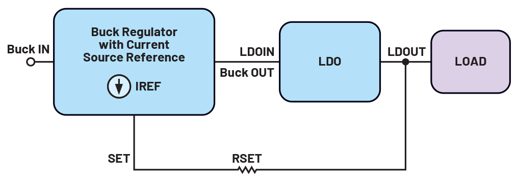
A key feature of this approach is that the SET pin can be referred to any voltage source, not just GND. This means the output voltage can be made to track another voltage, such as the output of a postregulator LDO, with an added offset defined by the RSET resistor. This flexibility is crucial for applications that require dynamically adjusting the output voltage while consistently maintaining the LDO voltage headroom.
For example, if the RSET resistor is connected to the output of the post-LDO seen in Figure 1, the output voltage of the buck regulator (Buck OUT) or the input voltage of the LDO (LDOIN) is determined as shown in Equation 1.

This configuration ensures that the buck converter dynamically adjusts its output to maintain a constant voltage headroom for the LDO, regardless of changes in the LDO output voltage (LDOOUT). This approach is ideal for applications where the LDO output is dynamically adjusted, as it helps sustain efficiency while preserving regulation performance. The voltage headroom is typically set by the system designer to achieve an optimal balance between the power supply rejection ratio (PSRR) and efficiency, depending on the application’s priority requirements. For instance, if the designer requires an LDO to be configured with a specific voltage headroom, then the SET resistor (RSET) should be chosen as shown in Equation 2.

The design configuration is especially robust. Even if the post-LDO output drops to zero or near zero due to overloading or a hard short to ground, the current source reference switching regulator will continue to maintain the voltage headroom above the LDO output. This ensures that the LDO remains biased and can recover once the fault is cleared. The headroom voltage should be set above the LDO’s minimum operating input voltage to ensure proper startup and allow recovery from fault conditions.
Figure 2 is another example that keeps the LDO above the minimum operating VIN by using a diode tied between the INTVCC and ISET pins.
The minimum voltage applied to the downstream LDO (LT3086) is determined by subtracting the forward voltage, Vd, of the diode (typically 0.7V) from the internal regulator voltage (INTVCC) regulation of the LTC3649, which is typically 3.45V. This results in an input voltage of approximately 2.75V for the LT3086.
However, since this LDO can operate with a minimum 1.4V input voltage, it is feasible to reduce the input voltage further without compromising regulator functionality. This can be achieved by adding a resistor, RINTVCC, in series with the diode as seen in Figure 3.
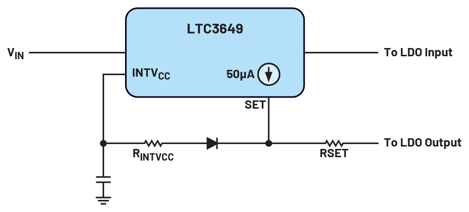
The value of the series resistor RINTVCC, used to adjust the desired minimum input voltage, Vmin, applied to the LDO, can be calculated using Equation 3.

As an example, the LDO headroom is configured to 0.5V (RSET = 10kΩ) with a minimum operating input voltage of 1.4V. The internal regulator voltage, VINTVCC, of the LTC3649 varies between 3.25V (min) and 3.65V (max). The minimum input voltage (Vmin) is set to 1.8V, providing sufficient margin to account for variations such as in VINTVCC, diode forward voltage drops, current source variations, and resistor tolerances. Then substituting the values into Equation 3 yields the RINTVCC value of 7.3kΩ.
From the E24 resistor series, a standard value of 7.5kΩ would be selected for RINTVCC to meet the target voltage requirements.
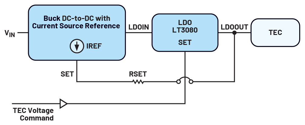
In Figure 4, the application involves a thermoelectric controller (TEC) that operates within a 0V to 9V range for temperature control, with the LDO output (LDOOUT) dynamically set based on a TEC command signal. The switching regulator can be a Silent Switcher® 3 (SS3) or any current source reference buck converter. This delivers low-noise performance from low frequencies up to the switching frequency range of the switching regulator.
Simulation and Test Results
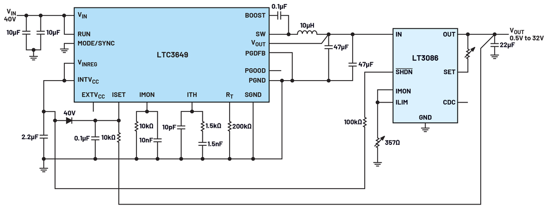
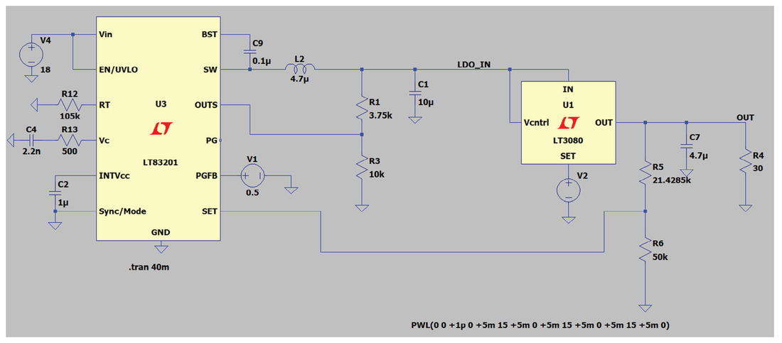
To demonstrate the proposed design approach, an LT83201, 18VIN, 1A SS3 step-down regulator was used for the buck converter while the LT3080, an adjustable 1.1A single resistor low dropout regulator, was used for the LDO. This is shown in Figure 5. This LDO is well-suited for precision voltage regulation and supports output voltages that can be adjusted down to 0V.
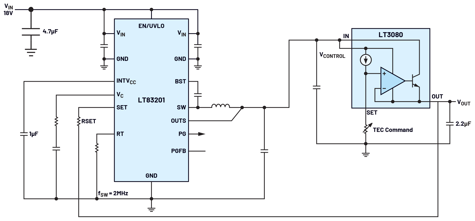
The LT3080 LDO requires a typical 1.35V VCONTROL to maintain proper output voltage regulation. To meet this requirement and ensure robust operation across this circuit’s conditions, the design in Figure 5 incorporates a voltage headroom of 1.5V between the LDO input and output voltage.
The RSET value is computed using Equation 4.

where IREF = 100µA for the LT83201.
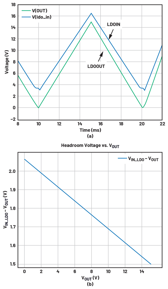
Figure 6 shows the simulation results between the output voltage and the input voltage of the LDO using LTspice®. Command voltage was applied to the SET pin of the LT3080, ramping from 0V to 9V within 5ms, followed by a ramp back down to 0V over the next 5ms. This simulates dynamic adjustment of the output voltage.
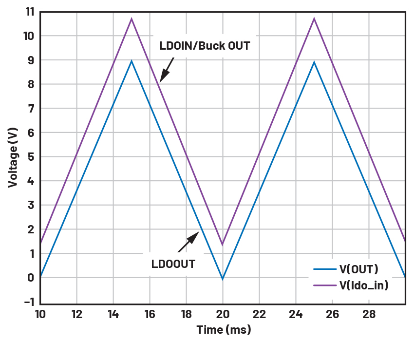
As shown in the simulation results, the LDO input voltage, which is connected to the buck regulator output, consistently tracks 1.5V above the output voltage. Stable regulation across the operating range can be maintained as long as the voltage headroom remains above the LDO’s minimum headroom requirement to avoid dropout.
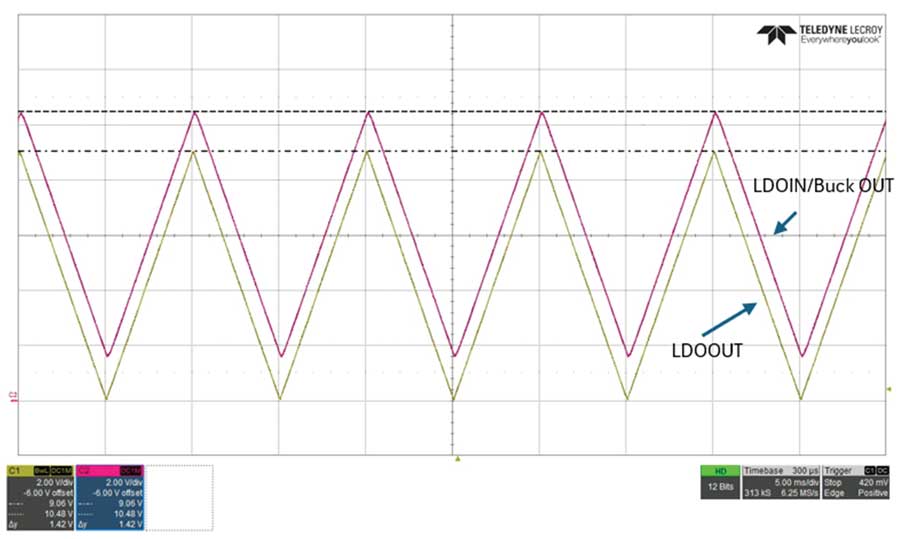
In addition to the simulation work, the design approach was also implemented using the EVAL-LT83201-AZ and DC995A to demonstrate the feasibility of the proposed concept. Throughout the test, the headroom was maintained at approximately 1.5V while the SET pin of the LT3080 was driven with a sawtooth waveform of 100Hz, cycling from 0V up to 9V, thereby representing the dynamic adjustability of the voltage headroom. This hardware demonstrates the approach beyond simulation and introduces practical methods for implementation. The test result is shown in Figure 7.
System Efficiency and Output Noise
One significant advantage of employing voltage headroom control for the LDO stage is the improvement in overall efficiency. In Figure 8a, this advantage is clearly visible in the system efficiency curves. The system with voltage headroom control (shown in blue) achieves higher overall system efficiency across the entire output voltage range, compared to the system without headroom control (shown in orange) where the switching regulator output remained fixed at 10.5V regardless of LDO output voltage. When the load is fixed at 1A (Figure 8b), the advantage of voltage headroom control becomes more evident. As shown in the graph, disabling voltage headroom control prevents the adjustable output voltage from being trimmed below 5V. The limitation occurs due to thermal constraints and the package dissipation limits of the LDO.
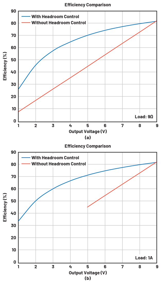
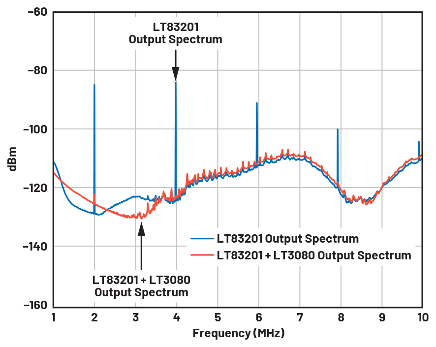
Figure 9 presents a comparison between the frequency output spectrum of a switching regulator with and without a post-LDO. The measurements are taken at the system output. The input voltage of the switching regulator is set to 18V, while the LDO output voltage is set to 1.8V with 500mA load current for both setups. The voltage headroom is set to 1.5V. As seen in Figure 9, the combination of a switching regulator and an LDO as a postfilter effectively attenuates both fundamental ripple and harmonic content. The LT3080’s high PSRR plays a crucial role in this noise reduction by filtering out ripple and its harmonics, resulting in a cleaner output voltage. This highlights a key advantage of using an LDO by suppressing switching noise while ensuring precise voltage regulation and good transient performance.
Design Considerations
It is important to observe the absolute maximum ratings of the switching regulator being used, particularly the SET and OUTS pins. For the LT83201, both pins have a maximum rating of 13V. This means the device can only be used if the combined voltage from the LDO output and its required headroom remains below 13V. Staying within these limits ensures the integrity of the design and prevents potential damage to the device. However, in systems that require a variable output voltage exceeding the absolute maximum rating of the SET and OUTS pins, one can implement a voltage divider network to scale down the voltage applied to the SET and OUTS pins as shown in Figure 10. This approach allows the main output voltage to operate at a higher level while ensuring that the SET/OUTS pins remain within their safe operating limits.
In the example design in Figure 10, the system requires 15V maximum output, but the LDO output of 15V must not be tied directly to the LT83201’s SET pin due to its absolute maximum (abs max) rating. Instead, the LDO output is first scaled down with a resistive divider, so the SET pin stays within the abs max rating. It is recommended to configure the SET pin voltage to be 12V at maximum output voltage, in which case the resistor values (R5 and R6) can be chosen according to Equation 5.

However, to ensure that the system can power up from 0V, the parallel combination of R5 and R6 multiplied by ISET must be equal to or greater than the required headroom voltage of the LDO. And to ensure that no rating is exceeded, it should be less than the absolute maximum rating of the SET pin. This is shown in Equation 6.

where Vheadroom is the minimum required LDO headroom voltage and SET (abs max rating) is the maximum voltage rating of the SET pin.
Combining both equations 5 and 6, R6 can be computed as shown in Equation 7.

In Figure 10, the design requires a headroom voltage of 1.5V, which means R6 can be calculated as 50kΩ. R5 can then be determined using Equation 5, resulting in a computed value of 21.43kΩ. A standard 22kΩ resistor can be used for R5.
After selecting the divider network of the SET pin, the divider network at the OUTS pin must be calculated. As stated in the LT83201 data sheet, it is recommended to choose the resistor values for R1 and R3 such that their impedance is less than 5kΩ to keep their noise contribution low compared to the noise contribution of the part itself. With this, assuming R3 is fixed at 10kΩ, the value of R1 can then be determined using Equation 8.

The result of the simulation is shown in Figure 11a. To ensure proper voltage regulation, a minimum load current must be maintained as indicated in the data sheet. In the case of the LT3080, at least 1mA of load current is required to keep the output stable across its operating conditions. However, note that as the output voltage decreases, the headroom voltage slightly increases as shown in Figure 11a. Since the divider network ratios for the SET and OUTS pins are not identical, this introduces a slight slope in the difference between the input and output voltage of the LDO, causing the headroom voltage to vary rather than remain constant across all output voltages as seen in Figure 11b. Nevertheless, this design consideration wherein the 1.5V headroom is set at the maximum output voltage ensures that the required LDO headroom is maintained under all output voltages.
Conclusion
This article demonstrates a simple yet effective method for managing LDO voltage headroom using current reference switching regulators. It allows for dynamic headroom control even when using LDOs that do not support the voltage input-to-output control (VIOC) function. By applying the voltage headroom control technique and validating the design through simulations, practical circuit implementations, and bench-tested data, the effectiveness of the solution was clearly established. The results showed a significantly cleaner output spectrum that reduces the fundamental output ripple and harmonics when using an LDO postfilter, while also offering a compelling strategy for precise voltage headroom control. As shown by actual measurements, the switching regulator output closely tracks the LDO output with a defined voltage offset, which can be precisely configured using a single resistor. It achieves a balance of efficiency and low noise across diverse output voltages, providing system engineers with efficient and low-noise power delivery systems. Additionally, for the use cases such as maintaining the LDO’s minimum operation voltage with low LDO output voltage conditions and keeping below the absolute maximum ratings on pins of current reference switching regulators in high LDO output voltage conditions, this article shows examples of circuitry workarounds.
About the Authors
Kyosuke Shimo joined Analog Devices Japan in 2022 as a new graduate and currently serves as a field applications engineer in the Industrial Customer Solutions Group. He supports power products and works closely with
Ino Lorenz Ardiente currently serves as a power architect engineer under the Power Solutions Group at Analog Devices Philippines. He holds a bachelor’s degree in electronic engineering from Pamantasan ng Lungsod ng Maynila
Aldrick S. Limjoco currently works as a senior manager, power architect under the Power Solutions Group at Analog Devices Philippines. Since joining ADI in 2006, he has taken on diverse engineering roles focused on power
Related to this Article
Products
RECOMMENDED FOR NEW DESIGNS
60V, 4A Synchronous Step-Down Regulator with Rail-to-Rail Programmable Output
RECOMMENDED FOR NEW DESIGNS
40V, 2.1A Low Dropout Adjustable Linear Regulator with Monitoring and Cable Drop Compensation
RECOMMENDED FOR NEW DESIGNS
18V, 1A Step-Down Silent Switcher 3 with Ultra-Low Noise Reference
Technology Solutions
Product Categories


