Circuit Suggestions using Features and Functionality of New Sigma-Delta ADCs-Part 1

Circuit Suggestions using Features and Functionality of New Sigma-Delta ADCs-Part 1
by
John Wynne
Oct 1 2001
Read other articles in this series.
In many modern cost-competitive markets from Field Instruments through Data Acquisition and on to Industrial and hand-held Instrumentation, there are pressures to both increase measurement throughput and to increase the functionality of designs by adding yet more features but at a lower cost. Some new and recently released Sigma-Delta ADCs from ADI offer a host of new and exciting features and sensor-excitation options that will challenge a designer's ingenuity to make use of them all.
- The AD7719 contains two Sigma-Delta ADCs, one with 24-bit resolution and one with 16-bit resolution, to allow simultaneous sampling of two analog input signals.
- The AD7708 and AD7718 are multichannel ADCs which allow users to select not only their optimum mix of differential and single-ended inputs, but also to select the most appropriate voltage reference for each channel.
- The AD7709 contains switchable matched current sources, low-side power switches, selectable reference sources plus a programmable front-end allowing a wide choice of analog inputs.
- The AD7740 is a Voltage-to-Frequency converter based on a first-order Sigma-Delta modulator. It is the world's smallest, lowest-cost 12-bit accurate VFC. It operates from 3 V or 5 V and offers high input impedance due to its input Buffer; the ADuC824 MicroController® is similar to the AD7719 but also contains an 8052 code-compatible core with 8 k bytes of FLASH/EE Code and 640 Bytes of FLASH/EE data space plus other peripherals such as a 12-bit DAC, time-interval counter, UART, serial I/O, and Watchdog Timer.
This white paper describes how the features and functionality of these devices can be used to solve everyday design tasks in a simpler and more cost-effective manner than ever before. The treatment of these different tasks is at a relatively high level, but it is hoped that the circuits presented here will fuel your own imagination into producing innovative solutions to your own problems, in your own style.
A. Indirect Temperature Measurement of a Bridge Transducer Permits Software Temperature Compensation.
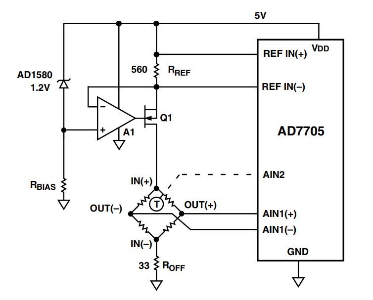
Bridge transducers are notorious for being sensitive to temperature. When the temperature changes almost everything varies in sympathy, some parameters going up and some going down. The temperature coefficient of span (TCS) is generally negative for piezo-resistive pressure sensors while the temperature coefficient of resistance (TCR) is positive. In other words, as the temperature rises the sensitivity decreases while the resistance of the bridge increases. In general, the TCS and TCR magnitudes are very close to each other. This has motivated to design engineers to add various external components, both active and passive, to achieve some measure of temperature compensation. However , calibration of these circuits can be tedious and the resultant performance problematic. Piezo-resistive bridge manufacturers have tried to equalize these coefficients in their manufacturing process to ease the problem. Another approach has been to simply measure the temperature of the bridge and use a microcontroller to compensate in software given certain basic data such as the bridge resistance at, 25C, and the TCR of the bridge. Figure A1 shows this approach. The symbol T represents some type of linear temperature sensor physically attached to the bridge. The bridge output is measured on differential channel AIN1 while the temperature sensor is measured on Channel AIN2. The bridge excitation current is determined by resistor R REF, voltage reference VREF, and op amp A1 in a standard circuit configuration to produce an excitation current equal to (VREF)/(R REF). This is a very effective approach but is hampered by concerns that the temperature measured may not be the real temperature of the bridge. For instance, placement of the temperature sensor vis-a-vis the mechanical attachment of the strain gauge will have a crucial bearing upon the accuracy of the reading. It would not be unusual to see errors of the order of a degree C or more in such situations. Whether this is important or not is a matter for the System Designer.
The idea presented here (and suggested by Reference A1) is the very simple one of measuring the temperature of the bridge by measuring the voltage developed across the bridge itself as a result of a known excitation current flowing through it. In Figure A2 three channels of the AD7708 are operated as pseudo-differential inputs, all with respect to AINCOM. When this input is tied to the midpoint of the bridge, it acts as a reference point from which to make all necessary measurements. The differential bridge output, seen between terminals OUT(+) and OUT(–), feeds directly into pseudo-differential channel AIN1/AINCOM of the AD7708. This can accept full scale signals as low as 20 mV.
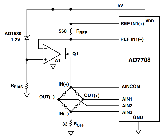
The voltage across the bridge is computed from the results of two additional measurements: input channel AIN2 measures the voltage from the top of the bridge to its midpoint (AINCOM terminal) while input channel AIN3 measures the voltage from the midpoint (AINCOM terminal again) to the bottom of the bridge. The voltage across the bridge can then be computed and from that computation the temperature of the bridge itself can be computed. It is assumed that the resistance of the bridge is independent of the pressure being measured, at least to the extent that it is immaterial to the measured results.
For these three measurements the AD7708 uses differential reference input pair REFIN1(+)/REFIN1(–) to derive its absolute reference from the voltage developed across precision resistor R REF. This voltage includes any offset error voltages due to A1. A circuit similar to this has been previously published in EDN [Reference A2].
This idea can be further pursued by using the AD7719 which has two sigma-delta ADCs on the same silicon and permits simultaneous conversion of two signals. Figure A3 shows this circuit where the current source of Figure A2 has been removed, thereby somewhat increasing the excitation voltage to the bridge. The differential input of the main 24-bit channel, AIN1/AIN2, along with its differential reference inputs, REFIN1(+)/ REFIN1(–), measure the bridge output ratiometrically.
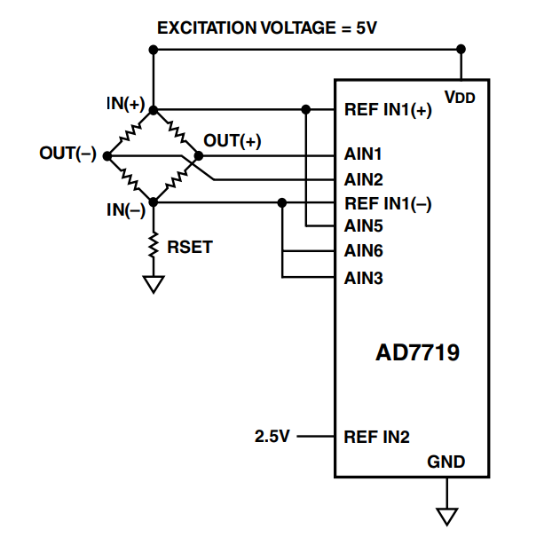
The auxiliary channel allows this ratiometric measurement to be translated back into absolute terms. Two channels are multiplexed into this 16-bit auxiliary ADC: differential pair AIN5/AIN6 measure the voltage across the bridge with respect to the absolute reference on it’s REFIN2 input while AIN3 measures the voltage across R SET to allow the absolute current through the bridge to be calculated, leading to the calculation of bridge resistance and hence bridge temperature.
B. Combining Absolute and Ratiometric Measurement Capability with One ADC.
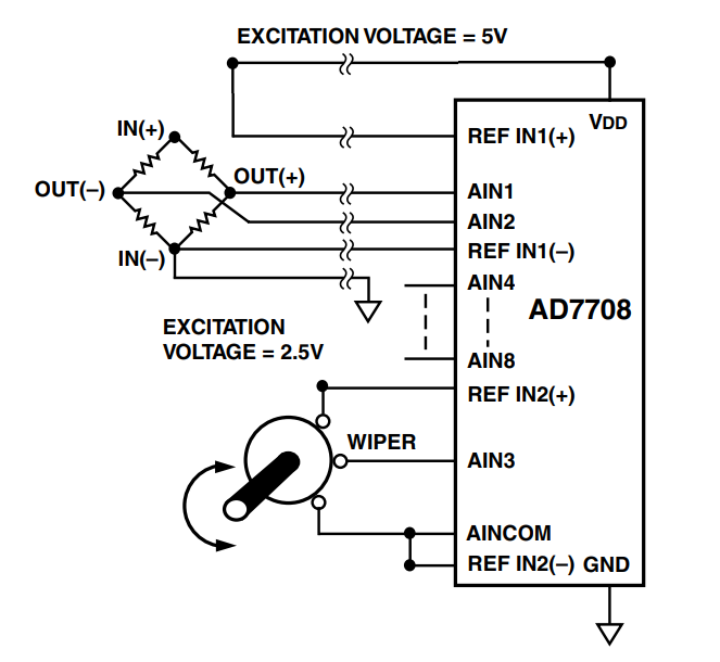
The AD7708, AD7718 and soon-to-be-released AD7709 have two independent sets of differential reference inputs. This allows users of a multichannel ADC to mix and match the channels they want to operate ratiometrically and those they want to operate in an absolute fashion. Figure B1 shows a remote bridge output being measured ratiometrically on differential input pair AIN1/AIN2, while the single-ended output of the local servo pot is being measured by single-ended input AIN3 using an absolute 2.5 V reference on the second set of reference inputs. The remaining channels (AIN4 to AIN8) can be configured as differential or single-ended inputs and can be converted with either reference pair.
Another example of mixing ratiometric and absolute measurements is shown in Figure B2 using the AD7709. This is a 16-bit ADC with a front-end 4-channel multiplexer. In addition it has two low-side power switches useful in power-sensitive applications to switch in and out sensors which may consume relatively heavy current. The example shows a bridge with its excitation being switched on and off as required via SW1/P1. If thermal settling of the bridge is an issue, then to allow for proper settling before taking a measurement. This is a ratiometric measurement with the reference pair, REFIN1(+)/REFIN1(–), across the entire bridge. Note that the IR drop across the SW1/P1 switch is eliminated by virtue of the differential reference input.
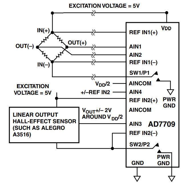
A second sensor, a linear output hall-effect sensor such as the A3516 from Allegro*, is shown connected to AIN3 and again is powered on and off as required by SW2/P2. Such a sensor typically produces an output signal of +/–2 V biased around VDD/2 in response to an applied magnetic field. Channel AIN3 can convert a unipolar or bipolar signal with respect to the voltage on AINCOM. By tying AINCOM to VDD/2, the full scale signal accepted by AIN3 is +/– REFIN(2)/2 or approximately +/–2.5 V biased around VDD/2, which is what's needed. Again note that any IR drops in SW2 are eliminated by virtue of the differential reference pair, REFIN2(+)/REFIN2(–). This is important since these types of sensors can take 10 mA of current introducing 10 mV of error for every 1 Ω of switch resistance.
C. Minimize Power Dissipation When Measuring Pt100s.
Multiplexing any number of 3-wire RTDs to a measurement system is straightforward and error-free only if the multiplexer error voltages, produced by the RTD excitation current flowing through the multiplexers’ on-channel resistance, are avoided. The circuit shown here demonstrates how any number of 3-wire Pt100s, the most popular form of RTD, can be monitored without the introduction of additional errors. Since the RTDs are considered local to the measurement system, the additional error sources of ohmic drops along the long wires is ignored.
Figure C1 shows 3 Pt100s being multiplexed into differential input AIN1/AIN2, one of two differential channels on the AD7709. This ADC has two low-side power switches that can be used to power-down the current excitation when no measurements are being made. Each Pt100 to be measured has associated with it two switches in a differential 4-channel multiplexer such as the ADG709. For instance, S1A and S1B are associated with RTD#1, S2A and S2B are associated with RTD#2, etc. The two switches associated with a particular RTD are either both open or both closed at any one time. Only one RTD can be measured at a time. The multiplexer control lines are not shown in the figure below to simplify the diagram.
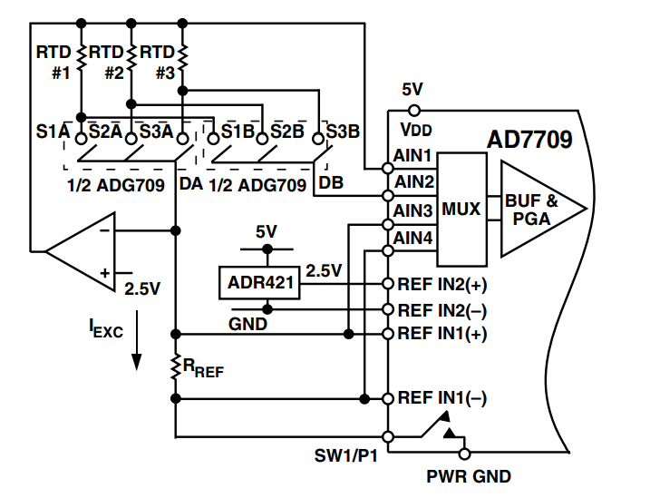
To measure RTD#1, switches S1A and S1B are closed and low-side power switch SW1/P1 is also closed. This allows the loop around op amp A1 to close by setting up a precision excitation current, IEXC, to flow through RTD#1, switch S1A, and the reference resistor R REF. For a Pt100, this current might be of the order of 5-10mA. To avoid seeing ohmic losses across S1A, the ADC uses S1B to monitor the RTD voltage directly across the RTD. It is important that no current flows through this monitoring switch. Consequently a requirement of the measuring ADC is that it has a buffered differential input, presenting a very high input impedance. The AD7709 has this buffer.
The input reference pair assigned to the RTD measurement is REFIN1(+)/REFIN1(–) and the reference voltage is the product of IEXC and R REF. Note that any IR drops across the low-side SW1/P1 power switch are eliminated by virtue of the differential reference input. As mentioned before in relation to hall effect sensors, a differential reference is important since these Pt100s can take 10 mA of current introducing 10 mV of error for every 1 Ω of switch resistance.
This is a ratiometric measurement since the value of the Pt100 excitation current depends not just on the precision 2.5 V reference (an ADR421 is very suitable here) applied to the noninverting input of A1, but also on the value of R REF, VOS of op amp A1, switch on-resistance of the ADG709, plus the on-resistance of SW1/P1. If it is necessary to transfer the readings to an absolute basis, then the second differential input channel and the second set of differential reference inputs can be used. The precision 2.5 V reference, used to set up the excitation current, is also applied directly to REFIN2(+)/REFIN2(–) while the second differential input AIN3/AIN4 measures the reference voltage for the first channel. This gives an absolute reading of what the reference voltage is for the first channel, allowing the RTD readings to be transferred to an absolute basis.
D. Eliminate Thermoelectric EMFS in Low-resistance Measurements.
When two metallic conductors made of different materials are joined together in a loop and one of the junctions is at a higher temperature than the other, then an electric current will flow through the loop. The magnitude of this current is dependent upon the type of metals involved and the temperature differential of the junctions. When such a loop is opened, a voltage a thermoelectric voltage will appear across the open ends. Again, this is dependent upon the type of metals involved and the temperature differential of the junctions.
When trying to measure very small signals or low impedances it is very possible to get errors in the readings due to thermal emfs. A standard way that DMM manufacturers have of dealing with such problems is to initially take one reading, reverse the excitation carefully, and then take a second reading. Averaging the two readings will eliminate the thermoelectric emfs from the final result. [Reference D1]
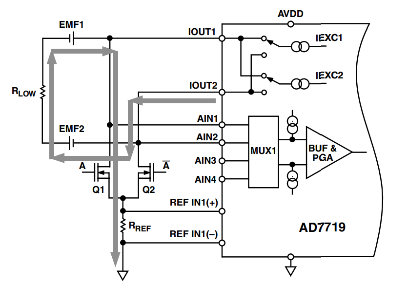
Figure D1 shows the AD7719 measuring a low-value resistor, RLOW. Also shown are two thermoelectric emfs, EMF1 and EMF2, representing summations of all the thermoelectric emfs encountered on the way out and on the way back between the ADC and the resistor. These would normally cause an error if a single measurement were taken of RLOW. However each of the AD7719’s two current sources, IEXC1 and IEXC2, can be programmed to appear at either of the package pins, IOUT1 and IOUT2. This allows the excitation current to be reversed through the low-value resistor thereby allowing two measurements to be taken and the effects of EMF1 and EMF2 to be eliminated.
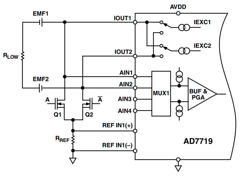
In order to increase the excitation and thereby increase the measurement sensitivity, the two internal 200 µA excitation currents are programmed to appear in parallel. Thus a single 400 µA current source is used as an excitation current, IEXC, in this application.
Transistors Q1 and Q2 steer the excitation current through the reference resistor, RREF, to ensure the same polarity reference voltage is always generated, regardless of excitation current direction. These transistors are driven in antiphase by Port pins P1 and P2 of the AD7719 (not shown in the diagram).
The current flow in each phase of a measurement is shown in Figures D2 and D3. During Phase 1 the excitation flows out of IOUT1 through RLOW and through RREF via Q2, to AGND. During Phase 2 the excitation currents flows out of IOUT2 through RLOW and through RREF via Q1, to AGND.
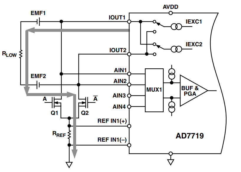
During Phase 1:
V Diff(Phase1) = V (AIN1) - V (AIN2)
= VEMF1 + VEMF2 + (I EXC)(RLOW)
Current sources are now switched during Phase 2:
V Diff(Phase2) = V (AIN1) - V (AIN2)
= VEMF1 + VEMF2 - (I EXC)(RLOW)
The two measurements are now combined in software to cancel thermoelectric EMFs:
V Diff = [V Diff(Phase1) – V Diff(Phase2)]/2
= (I EXC)(RLOW)
Finally this ratiometric measurement is turned into an absolute one. This is achieved by configuring two more of the AD7719 analog inputs, AIN3 and AIN4, as a second differential input into the main 24-bit ADC channel and driving them with an absolute voltage reference such as an ADR421. Taking a reading of this known voltage but with an "unknown" reference allows a design engineer to infer the unknown reference value and hence the absolute value of V Diff on AIN1/AIN2.
E. For TEC Applications, Implement Your Own Mix of Analog Input and Output Channels.
In modern Thermoelectric Cooler (TEC) applications — found especially in the optical communications industry —numerous A/D and D/A channels are required to measure and control laser diode parameters like temperature, current, set limits, and flags. Low-cost string DACs such as the AD5304/AD5314/AD5324 family of quad 8-, 10- and 12-Bit Resolution DACs are very popular for these duties. Nevertheless, sometimes one or two particular tasks require more resolution than these DACs offer. Consequently, designers are forced to specify a generally more expensive DAC to meet this high resolution requirement. This can be accoplished by scaling the outputs of two DACs and subsequently summing them together to produce a composite higher-resolution DAC output.
To ensure the circuit is operating as intended , i.e, (the correct code was loaded to the correct DAC?), the composite output voltage should be monitored by an ADC with even higher resolution than the composite DAC. If the ADC being used in this TEC application is a multichannel high-resolution ADC and you’ve got at least one spare ADC channel is available, then this channel can be used to monitor the composite output voltage.
The AD7708 shown in Figure E1 is operating in its 10-channel mode and uses a single set of differential reference inputs, REFIN1(+)/REFIN1(-), for all 10 channels. Channel AIN1 is dedicated to the composite output voltage while the other nine channels could either be used as ADC channels or some of them could be dedicated to monitoring other composite DAC outputs. Thus it is possible to tailor a system to meet most requirements.
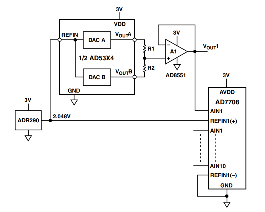
In Figure E1 the DAC A and DAC B channels of the quad 10-bit resolution DAC, the AD5314, are summed together to produce VOUT1. Scaling resistors R1 and R2 have a 15:1 ratio to provide a composite LSB size of 1/15 the normal 10-bit LSB size.
With R1 = 15R2, the output voltage is expressed as
VOUT1 = (VOUTA/16) + (15.VOUTB/16)
VOUT1 = VREF[(DA/16) + (15DB/16)]
where DA and DB are fractional representations of the digital words in DAC registers A and B, respectively (0</= DA</= 1023/1024, 0</= DB </= 1023/1024).
A reference voltage of 2.048 V is generated by the ADR290 and feeds both the AD5314 DAC and AD7708 ADC. All components work off of 3 V including the low-noise, low-offset drift op amp AD8851.
DAC B is the Most Significant (MS) or dominant DAC with an effective composite LSB size of 1.875 mV, while DAC A is the Least Significant (LS) DAC and has an effective composite LSB size of 125 μV. The composite DAC thus has an LSB size equivalent to a 14-bit resolution DAC. Under these conditions the AD7708 will deliver an exact picture of the composite output voltage level with a resolution of 30 μV. Choosing different R1/R2 scaling will produce a different composite output voltage. Note as a general rule that all single-supply DACs have reduced current-sink capability at output voltages near 0 V. Thus, it is recommended that the very lowest DAC codes be avoided.
References
Reference A1; “Temperature Compensating an Integrated Pressure Sensor” by Bruno Paillard, Sensors, January 1998, p36 – p48.
Reference A2; “Bridge-temperature measurement allows software compensation” by John Wynne, EDN, August 17, 2000, pgs. 127-128.
*Allegro Microsystems, Worcester, MA, https://www.allegromicro.com
Reference D1; “Low Level Measurements”, Keithley, 5th Edition