Overview
Design Resources
Design & Integration File
Download Design Files 9.72 MEvaluation Hardware
Part Numbers with "Z" indicate RoHS Compliance. Boards checked are needed to evaluate this circuit.
- EVAL-CN0554-RPIZ ($153.81) ±10 V Analog Input and ±15 V Analog Output for Raspberry Pi Platforms
- EVAL-CN0556-EBZ ($287.50) Programmable High Current and Voltage Source/Sink Power Supply
Features & Benefits
- High Efficiency Buck or Boost DC-DC Converter
- 14 V to 56 V Buck Input Voltage and 8 V to 14 V Boost Input Voltage
- Fully Programmable Bidirectional Control and Monitoring
- Seamless Buck-to-Boost Transition and Vice Versa
- Buck Mode: 35 A Maximum Output Current
- Boost Mode: 10 A Maximum Output Current
- Undervoltage, Overvoltage, Overcurrent, and Reverse Current Protection
Parts Used
Documentation & Resources
-
EVAL-CN0556-EBZ User Guide (GitHub)4/16/2026
-
CN0556: Programmable High Current and Voltage Source/Sink Power Supply (Rev. 0)12/22/2023PDF813 K
Circuit Function & Benefits
Test and instrumentation applications such as battery formation, power supply testing, and lighting applications require precise control of voltage and current, often with bidirectional power flow. Battery formation requires multiple charging and discharging cycles; particularly, during the discharge cycle where the battery provides power to the input supply. LED applications require both voltage and current-mode operation at the device under test (DUT). Reverse- power applications require voltage and current limit at both the input supply and DUT.
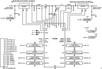
The circuit shown in Figure 1 is a programmable buck or boost power supply featuring an adjustable buck output of 2 V to 14 V, 35 A, and adjustable boost output of 14 V to 56 V, 10 A. The design allows the mode of operation to be externally controlled or automatically selected. Six independent control loops regulate input and output voltage in both directions, as well as provide input and output current limit programming and monitoring.
The solution contains input and output protection MOSFETs to protect against negative voltages, control inrush currents and provide isolation between terminals under fault conditions such as switching MOSFET shorts. Internal and external fault diagnostics and reporting are available to improve the reliability of the system from a safety perspective.
The system input and output voltages and currents are monitored and controlled through an analog I/O module. Through this, a single board computer such as a Raspberry Pi platform can receive telemetry information to control the board remotely.

Circuit Description
The core of the CN0556 is the LT8228 bidirectional synchronous 100 V buck/boost controller with reverse supply, reverse current, and fault protection. The CN0556 controls the flow of power between a higher voltage (V1) and a lower voltage (V2), functioning as a synchronous buck and converter.
The CN0556 allows six different control modes. For both buck and boost regulator directions, it can either be in a constant-voltage output, constant-current input, or constant-current output for both buck and boost directions. The device operates on which of the three limits it reaches first. The board can be set to buck or boost mode via the DRXN pin controlled through a digital signal from the host or by configuring the pin for auto-selection.
BUCK MODE OPERATION
In buck mode, the LT8228 is a peak current mode step-down controller where V1 is the input supply and V2 is the output load.
Setting the Buck Output Voltage
V2D is the node to be regulated by the internal circuitry of the LT8228 through the V2 output voltage control block connected from V2D to the FB2 feedback pin, as shown in Figure 1. The internal reference voltage of 1.21 V and the ratio of the resistor divider network controls the output voltage of the buck regulator.
The CN0556 has a regulated V2D output voltage range of 2 V to 14 V by setting RFB2A and RFB2B to 12.7 kΩ and 1.21 kΩ, respectively. Figure 2 shows the dynamic control of the output voltage by using the control resistor RFB2_CTL. Injecting the external control voltage FB2_CTL to the RFB2_CTL resistor forces an additional current to RFB2B making the LT8228 regulator pull the output voltage down according to Equation 1. From this, the CN0556 has a regulated V2D output voltage range of 2 V to 14 V. Note that the output voltage is at maximum when FB2_CTL is set at 1.21 V

The output voltage is calculated using Equation 1:

Where:
V2D = buck output voltage
FB2_CTL = control voltage
Note that it is possible not to use the full 1.21 V to 10 V input voltage control range to set the buck output voltage within its 2 V to 14 V output.
Setting the V1 Buck Input Undervoltage
In buck mode, the LT8228 has V1 input undervoltage detection at the UV1 pin. The default V1 input undervoltage threshold of CN0556 is set at 54 V through the ratio of two resistors, RUV1A and RUV1B, as shown in Figure 3.

CN0556 features an external undervoltage threshold control wherein a voltage ranging from 1.21 V to 10 V can be injected to RUV1_CTL resistor from analog module/controller. This allows the threshold to be adjusted from 12 V to 54 V and be computed using Equation 2. Note that after the undervoltage thresholds have triggered, the overvoltage thresholds increase by 100 mV typically. Similar to the output voltage feedback pin FB2, the undervoltage input pin UV1 regulates the voltage at the pin to 1.21 V. This programmatically sets the buck input undervoltage from 12 V to 54 V. The undervoltage control threshold is set using Equation 2:

Where:
VUV1 = buck input undervoltage threshold for V1
UV1_CTL = control voltage
Note that the input control voltage must range only from the minimum 1.21 V up to n volts, where VUV1 will just be up to the designed 12 V minimum undervoltage threshold.
Setting the Buck Input and Output Current Limits
The current limit at both the buck input and buck output can be dynamically set when an external voltage ranging from 1.21 V to 10 V is injected into the ISET1P_CTL and ISET2P_CTL pins through a control resistor each added to the ISET1P and ISET2P pins. The control voltages dynamically set the current limit threshold from 0.07 A to 10 A at the buck input and from 0 A to 35 A at the buck output, as shown in Equation 3 and Equation 4. As depicted in Figure 4, connecting a resistor R1P from ISET1P to ground programs the V1 buck input current limit.


Where:
I1P = buck input current limit
ISET1P_CTL = control voltage
Similarly, the V2 buck output current limit is controlled by connecting a resistor R2P from the ISET2P pin to ground, as shown in Figure 5. Placing a parallel capacitor to R1P and R2P ensures that the current limit is set to the desired average current. The parallel capacitors also reduce the ripple voltage at the ISET1P and ISET2P pins and reduce the duty cycle jitter due to noise.


Where:
I2P = buck output current limit
ISET2P_CTL = control voltage
The ISET1P pin generates an output current that is proportional to the current passing through the sense resistor RSNS1. Similarly, the ISET2P pin generates an output current proportional to the current passing through RSNS2. During the current limit, the LT8228 regulates the voltage at the ISET1P and ISET2P pins to the internal reference voltage of 1.21 V.
Setting R1P to 90.9 kΩ programs the V1 buck input current limit to 10 A, while setting R2P to 187 kΩ and connecting to ISET2P programs the V2 buck output current limit to 35 A.
Note that it is possible not to use the full 1.21 V to 10 V input voltage control range to set the input and output buck current limits within its specifications.
Buck Mode Specifications Summary
| Symbol | Parameter | Conditions | Min | Typ | Max | Unit |
| V1 | Input Voltage | 14 | 56 | V | ||
| UV1 | Undervoltage Threshold | 12 | 54 | V | ||
| V2 | Output Voltage | where V1 ≠ V2 | 2 | 14 | V | |
| Output Current | 35 | A | ||||
| fsw | Operating Frequency | 145 | kHz |
BOOST MODE OPERATION
In boost mode, the LT8228 is a peak current mode step-up controller where V2 is the input supply and V1 is the output load.
Setting the Boost Output Voltage
In boost mode, V1D is the node to be regulated by the internal circuitry of the LT8228 through the V1 output voltage control block connected from V1D to the F1B feedback pin, as shown in Figure 6. Similar to the control circuitry in buck mode, the internal reference voltage of 1.21 V and the ratio of the resistor divider network controls the output voltage of the boost regulator at the V1 side.

The CN0556 has a regulated V1D output voltage range of approximately 14 V to 56 V by setting RFB1A and RFB1B to 54.9 kΩ and 1.21 kΩ, respectively. Regulating the FB1 feedback pin to 1.21 V makes the current set by the resistor connected to the ground constant. Similar to the resistor voltage feedback network in the Buck Mode section, the dynamic control of the output voltage by using the control resistor RFB1_CTL. Injecting a voltage greater than 1.21 V into the RFB1_CTL control resistor forces an additional current to the bottom resistor making the LT8228 regulator pull the output voltage down proportional to the input control voltage ranging from 0 V to 10 V. The boost output voltage can be calculated using Equation 5.

Where:
V1D = boost output voltage
FB1_CTL = control voltage
Setting the V2 Boost Input Undervoltage
In boost mode, the LT8228 has an input undervoltage detection at the UV2 pin. Similar to the undervoltage threshold ability of the regulator in buck mode, it can be controlled using the ratio of two external resistors RUV2A and RUV2B. Setting RUV2A and RUV2B to 10 kΩ and 1.21 kΩ, respectively sets the V2 boost input undervoltage to 12 V. The boost input undervoltage threshold also has a control feature in which, when an external voltage ranging from 1.21 V to 10 V is injected into RUV2_CTL. The undervoltage input pin UV2 is also regulated to the internal voltage reference of 1.21 V. This programmatically sets the boost input undervoltage from 8 V to 12 V.

The undervoltage control threshold for the boost input is calculated using Equation 6:

Where:
VUV2 = boost input undervoltage threshold for V2
UV2_CTL = control voltage
Note that the input control voltage must range only from the minimum 1.21 V up to n volts where the VUV2 will just be up to the designed 8 V minimum undervoltage threshold.
Setting the Boost Input and Output Current Limits
The dynamic configuration of current limits at both the boost input and boost output is achievable by injecting an external voltage, ranging from 1.21 V to 10 V, into the ISET1N_CTL and ISET2N_CTL pins. Each of these control voltages is applied through a control resistor to the ISET2N and ISET1N pins setting the current limit threshold, ranging from 0 A to 35 A at the boost input and 0.07 A to 10 A at the boost output, as described in Equation 7 and Equation 8.
Similar to the current control programming in buck mode, connecting a resistor R2N from ISET2N to ground programs the V2 boost input current limit, as depicted in Figure 8.


Where:
I2N = boost input current limit
ISET2N_CTL = control voltage
Similarly, the V1 boost output current limit is controlled by connecting a resistor R1N from the ISET1N pin to ground, as shown in Figure 9.


Where:
I1N = boost output current limit
ISET1N_CTL = control voltage
Placing a parallel capacitor to R1N and R2N ensures that the current limit is set to the desired average current. The parallel capacitors also reduce the ripple voltage at the ISET1N and ISET2N pins and reduce the duty cycle jitter due to noise.
Similar to buck mode, the ISET1N pin generates an output current that is proportional to the current passing through the sense resistor RSNS1 at the boost output side V1. Similarly, the ISET2N pin generates an output current proportional to the current passing through RSNS2. During the current limit, the LT8228 regulates the voltage at the ISET1N and ISET2N pins to the internal reference voltage of 1.21 V.
Setting R2N to 187 kΩ and connecting to ISET2N programs the V2 boost input current limit to 35 A, while setting R1N to 90.9 kΩ programs the V1 boost output current limit to 10 A.
Note that it is possible not to use the full 1.21 V to 10 V input voltage control range to set the input and output boost current limits within its specifications.
Boost Mode Specifications Summary
Table 2 shows the summary of performance when CN0556 is operating in boost mode.
| Symbol | Parameter | Conditions | Min | Typ | Max | Unit |
| V2 | Input Voltage | 10 | 14 | V | ||
| UV2 | Undervoltage Threshold | 8 | 12 | V | ||
| V1 | Output Voltage | where V1 ≠ V2 | 14 | 56 | V | |
| Output Current | 10 | A | ||||
| fsw | Operating Frequency | 145 | kHz |
SWITCHING MOSFET OPERATION
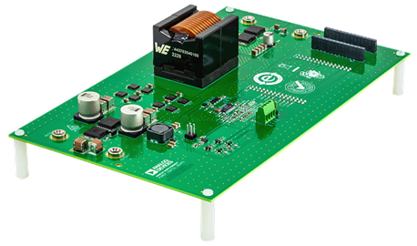
The CN0556 is equipped with top and the bottom switching MOSFETs M2 and M3, which are a combination of eight MOSFETs configured in series and parallel connections — designed to further optimize the supply to meet the current and thermal requirements. The breakdown voltage of the switching MOSFETs M2 and M3 have been appropriately selected considering the maximum input voltage of the system that will pass through them.
During buck mode, where V1D represents the input voltage and V2D the output voltage, M2 serves as the main switch; and M3 operates as the synchronous switch. Conversely, in boost mode, with V2D as the input voltage and V1D as the output voltage, M3 functions as the main switch; while M2 acts as the synchronous switch.
INPUT AND OUTPUT PROTECTION
Protection MOSFETs are placed in between the V1 terminal and the V1D input of the regulator and in between the V2 terminal and V2D. These are used to protect the regulator from reverse current, negative voltages, inrush currents, and also to provide isolation between the high side and low side parts of the regulator during fault conditions in both buck and boost modes.
V1 Protection MOSFET Controller Operation
The LT8228 provides protection functionality at the V1 terminal using two N-channel MOSFETs M1A and M1B connected back-toback in series, as shown in Figure 10.

In this configuration, DS1 is the source and DG1 is the gate of both M1A and M1B. V1D is the drain of M1A and V1 is the drain of M1B.The advantages of the dual MOSFET configuration are inrush current control and complete isolation of the V1 terminal in a fault condition. In normal operation, the controller drives DG1 high with a typical 10 μA pull-up current that enhances the V1 protection MOSFETs to provide a low loss conduction path between V1 and V1D. The DG1 voltage is clamped at a typical value of 10 V above DS1.
In buck mode, M1A is used by the LT8228 to protect the regulator from reverse current from V2 to V1 and possible negative voltages on V1, and M1B is used to control inrush current from V1 to V1D and to also provide isolation between V1 and V2 during fault conditions. This protection feature is useful for applications where V2 is pre-biased with a load such as a battery.
In boost mode, M1A is used to protect the output of the boost regulator from negative voltages on V1 and to control the outrush current from V1D to V1 and M1B is used to control the inrush current from V1 to V1D and also to provide isolation between V1 and V2 when a fault is triggered.
V2 Protection MOSFET Controller Operation
For V2 terminal protection, the LT8228 uses two N-channel MOSFETs M4A and M4B connected back-to-back in series, as shown in Figure 11. In this configuration, DS2 is the source and DG2 is the gate of both M4A and M4B. V2D is the drain of M4A and V2 is the drain of M4B.

The advantages of dual MOSFET configuration are inrush current control in boost mode and complete isolation of the V2 terminal in a fault condition. In normal operation, the controller drives DG2 high with a typical 10 μA pull-up current that enhances the V2 protection MOSFETs to provide a low loss conduction path between V2 and V2D.
The DG2 voltage is clamped at a typical value of 10 V above DS2. The DG2 controller shorts DG2 to DS2 thereby isolating V2 from the rest of the circuit when the LT8228 is disabled, or the internal temperature rises above the overtemperature threshold.
MODE OF OPERATION (DRXN)
The CN0556 can be set to buck or boost mode via the DRXN pin either by controlling it through a digital signal from the host or by configuring the DRXN pin for auto-selection. To operate the board in buck mode, the pin must be pulled HIGH and pulled LOW to select the boost mode operation.
It is also possible for the DRXN to auto-select the mode of operation based on the UV1, UV2, FB1, and FB2 pin voltages. If UV1 pin voltage is greater than 1.2 V, the board is in buck mode but if UV1 goes lower than 1.2 V, it is operating in boost mode. The LT8228 can also change its mode from buck to boost automatically if the UV1 pin voltage drops below 1.2 V or if the pin voltage at FB2 stays higher than 1.3 V for a certain number of cycles.
Similarly, the CN0556 can shift from boost to buck mode if the UV2 pin voltage drops below 1.2 V or if the FB1 pin voltage stays higher than 1.3 V at a certain period.
FAULT DETECTION AND REPORTING
The LT8228 provides a serial data stream with fault data. This device can check its internal circuit blocks, external MOSFETs, as well as several fault conditions including undervoltage and overvoltage faults. The stream is continuous, not conforming to a standard interface available on the Raspberry Pi. As such, a local Teensy processor captures and interprets the report data, which is forwarded to the Raspberry Pi over asynchronous serial communication.
The LT8228 continuously reports a 32-bit word at the active low REPORT pin using the SYNC pin as the data clock. To read from the REPORT pin, a clock signal with similar frequency as the board must be run through the SYNC pin, otherwise the REPORT pin will remain high impedance. The SYNC serves as the data clock in reading the REPORT data stream. Figure 12 shows the data read from the REPORT pin when the board was subjected to an undervoltage fault, with a 145 kHz clock signal into the SYNC pin.

CN0556 SYSTEM DIAGNOSTICS
By interfacing the CN0556 with an analog I/O module such as the CN0554, and a single computer such as a Raspberry Pi, full control and monitoring of the input and output voltages and currents can be performed.
The parameters to be monitored are translated and scaled to 0 V to 2.5 V range to match the input of the analog-to-digital converter (ADC) of the analog I/O module.
Voltage Monitoring
As shown in Figure 13, the input and output voltages are measured using a resistor voltage divider and the ADA4505 buffer amplifier.

The resistor voltage divider scales the buck input and boost output voltage at the V1 side from 14 V to 56 V and the boost input from 10 V to 14 V and the buck output voltage from 2 V to 14 V, to the ADC input voltage range. A summary of the measured parameters is shown in Table 3.
| Parameter | Divider Scale Factor | |
| V1_ADC | Buck Input Voltage, Boost Output Voltage | 25.3 V/V attenuator |
| V2_ADC | Buck Output Voltage, Boost Output Voltage | 6.1 V/V attenuator |
Current Monitoring
The circuit provides input and output current monitoring using the IMON1 and IMON2 pins. For reading the current at the V1 side, the current output of IMON1 is scaled to the voltage across the current sense resistor RSNS1 divided by the input sense resistor RIN1, as described in Equation 9:

The current flowing out of IMON1 is a scaled representation of the V1 input current in buck mode and V1 output current in boost mode. Likewise, the current exiting IMON2 is the scaled to voltage across the current sense resistor RSNS2 divided by its input sense resistor RIN2,which then represents the V2 output current in buck mode and V2 input current in boost mode.
Connecting resistors RMON1 and RMON2 from these pins to ground generates a voltage VMON1 and VMON2, respectively, available for monitoring by an external ADC.
To align with the 2.5 V input specification of the external ADC, RMON1 and RMON2 are selected to be 187 kΩ and 53.6 kΩ, respectively. The VMON1 and VMON2 voltages are read by the ADC without any amplification or attenuation at all.
The current values are calculated from the VMON1 and VMON2 voltage using Equation 10 and Equation 11, respectively:

Where:
IV1 = buck input current / boost output current
VMON1 = voltage proportional to IMON1

Where:
IV2 = buck output current / boost input current
VMON2 = voltage proportional to IMON2
POWER ARCHITECTURE
The LT1930, a step-up DC/DC converter boosts 5 V from the external supply to 12 V, which is used as input to the BIAS pin of the LT8228. This pin supplies the DRVCC regulator as well as the internal control circuitry. BIAS is connected to V1, V2, or an external supply via a diode OR circuitry. This configuration provides maximum current capability and decreases power loss at the DRVCC pin, which may cause current limit fold back.
The LT3010 low dropout regulator steps down the voltage at the BIAS pin to provide the 3.3 V supply to two ADA4505 single micropower amplifiers, which will be used by the analog I/O module to monitor the output voltages at V1 and V2 terminals. Figure 14 shows the power tree of the CN0556.

SYSTEM PERFORMANCE
Load Regulation
For a power supply, load regulation is a parameter that shows how well the output voltage stays constant with respect to changes or fluctuations in load current. Figure 15 shows that the load regulation of the CN0556 in buck mode is within 40 mV as the output load current is increased from 0 A to almost 35 A.

In boost mode, the regulation is within 8 mV when the output load current is increased from 0 A to 7 A, as shown in Figure 16.

Thermal Performance
Figure 17 and Figure 18 show the temperature change of the CN0556 when placed under its maximum limits for more than one hour at 25℃ room temperature.
In buck mode, the maximum temperature of the LT8228 is 90.3°C at 56 V input, 2 V to 30 A output current-limit.

In boost mode, LT8228's maximum temperature is 90.9°C at 14 V input, 30 A input current-limit, and 56 V, 4 A output load. Both thermal readings are well below LT8228's maximum operating temperature of 125°C.

Power Supply Efficiency
Figure 19 shows the efficiency of the converter when set to operate in buck mode, with 56 V input and a typical output voltage of 14 V.

Figure 20 shows the efficiency of the converter when set to operate in boost mode, with 14 V input and a typical output voltage of 56 V.

Common Variations
The LT8228 enables a masterless fault-tolerant mechanism for sharing output current among multiple LT8228s operating in parallel. This arrangement allows for increased load current, improved heat distribution, and redundancy. Since each LT8228 regulates to the average output current, the need for a master controller is eliminated. When an individual LT8228 is disabled or in a fault condition, it stops contributing to the average bus, making the current sharing scheme fault tolerant. This functionality is achieved through the utilization of the LT8228 ISHARE and IGND pins. When multiple LT8228s are paralleled, all DRXN pins are tied together to operate all LT8228s in the same regulation mode.
The LT8708 is an 80 V synchronous 4-switch buck-boost DC/DC controller with bidirectional capability similar to the LT8228. The LT8708 is a high-performance regulator that can operate at an input voltage that can be above, below, or equal to the output voltage.
The forward input, reverse input, forward output, and reverse output current limits can be set independently using four resistors on the board.
Circuit Evaluation & Test
This section covers the setup and procedure for evaluating the EVAL-CN0556-EBZ. The test features the use of the EVALCN0554- RPIZ analog I/O module since this board is designed to attach with a Raspberry Pi platform and is compatible with the CN0556.
For complete details on getting the system running, check the CN0556 User Guide.
EQUIPMENT NEEDED
Required Hardware
- EVAL-CN0556-EBZ
- Analog I/O module (EVAL-CN0554-RPIZ)
- Raspberry Pi 4 model B
- Raspberry Pi USB-C power supply
- Benchtop power supply, up to 56 V and 35 A
- Digital multimeter
- Electronic load
- MicroHDMI to HDMI cable
- Monitor with HDMI display
- USB keyboard and mouse
- 16 GB microSD Card
Required Software
- Analog Devices, Inc. Kuiper Linux image
- Python 3.7 or newer
GETTING STARTED
- Configure the microSD Card with Kuiper Linux for the CN0556 by following the instructions in the CN0556 User Guide.
- Insert the microSD card into the Raspberry Pi's SD card slot.
- Connect the CN0556 on top of the CN0554 and Raspberry Pi combination based on Figure 21.
- Connect the HDMI cable from the Raspberry Pi to the display monitor, and then connect the keyboard and mouse to the USB ports.
- Plug the USB Type-C power adapter into the Raspberry Pi and wait for it to boot up.

SETUP AND TEST
By default, the board is set up for buck mode operation. To perform the evaluation test, follow below steps:
- Turn on the power supply and the electronic load.
- Set the power supply at V1 to 56V, and set the current limit to 2 A.
Note: Do not enable the power supply output yet.
- Set the electronic load at V2 terminal to 0.1 A, and then enable the electronic load.
- Open a terminal and run the example script. The script is set to regulate the output to 14 V.
- The details of the current and voltage set at the output will be displayed.
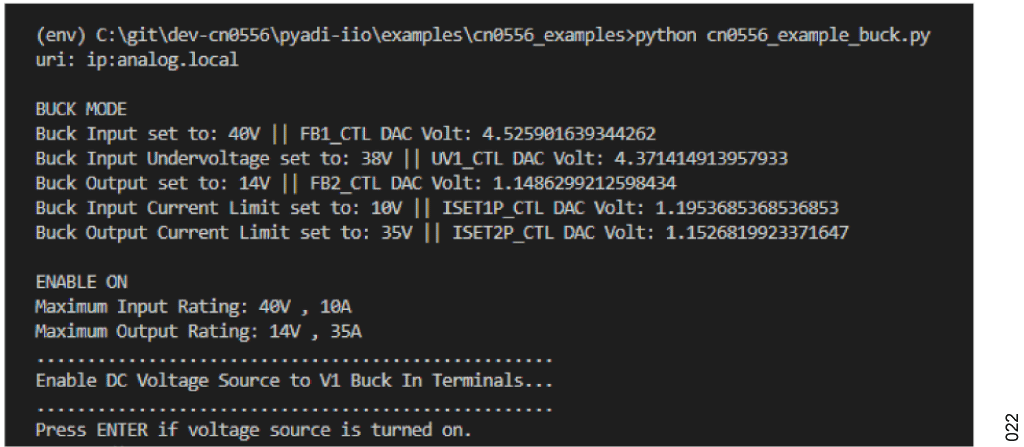
- Enable the output of the power supply into the V1 terminals.
- Verify that the voltage reading at the DMM is 14 V. Adjust the voltage at the power supply accordingly to set the output to 14 V. Take note of the undervoltage and overvoltage values when setting the supply. Make sure to return the input power supply to 56 V after the adjustment, then press the ENTER key to continue.
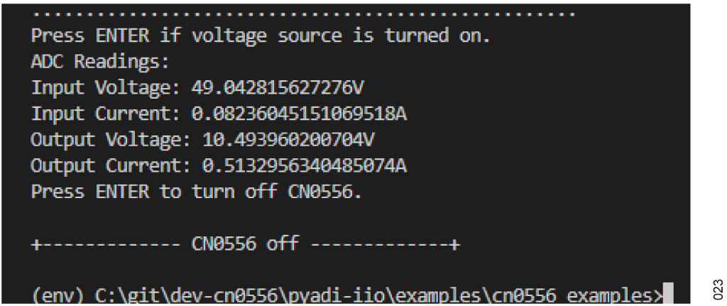
- The input and output voltage and current at the V1 and V2 will be printed in the terminal. The board will continuously regulate the output voltage to 14 V unless CN0556 is turned off.
For Boost Mode test setup, check the CN0556 User Guide.


