Overview
Design Resources
Design & Integration File
- Schematic
- Bill of Materials
- Gerber Files
- Allegro Layout File
- Assembly Drawing
- LTspice Simulations
Evaluation Hardware
Part Numbers with "Z" indicate RoHS Compliance. Boards checked are needed to evaluate this circuit.
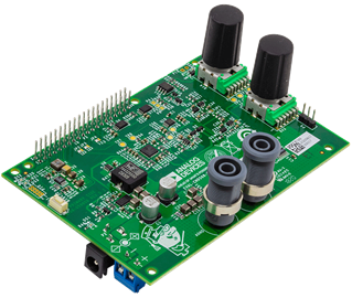
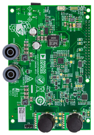
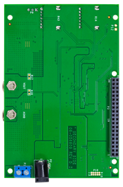
- EVAL-CN0508-RPIZ ($155.66) Software Controllable 75W Benchtop Power Supply
Device Drivers
Software such as C code and/or FPGA code, used to communicate with component's digital interface.
AD5686 GitHub Linux Driver Source Code (SPI)
nanoDAC+ GitHub no-OS Driver Source Code
Features & Benefits
- 75 Watt Power Supply
- Constant Current (>3A) and Constant Voltage (>25V) Modes
- True 0V and 0A operation
- Manual or Software Controlled
Product Categories
Markets and Technologies
Parts Used
Documentation & Resources
-
CN0508 User Guide5/24/2021WIKI
-
Solutions For Rapid Prototyping: Answering the Needs of Practicing Engineers8/23/2023PDF784 K
-
CN0508: 75 Watt, Single-Output Benchtop Power Supply (Rev. 0)6/1/2020PDF393 K
Circuit Function & Benefits
A high-quality benchtop power supply is an essential piece of equipment in any electronics or science laboratory because when power integrity is compromised, sensitive circuits can fail in unexpected ways. However, most of the power supplies on the market today offer competitive specifications at the expense of high cost, size, and heat dissipation.
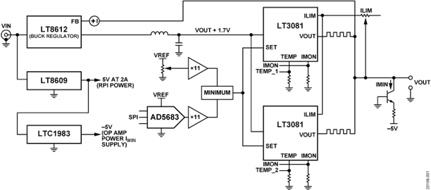
The circuit shown in Figure 1 is a single-channel, 75 W benchtop power supply featuring an adjustable wide output voltage range of 0 V to 27.5 V and current limiting/constant current operation (up to 3 A).

With a Raspberry Pi®-compatible expansion header, electronic control through either a local touchscreen or over a wireless or wired network connection is possible. Output voltage can be controlled manually or by software, and a manual current-limit control sets the transition from constant voltage to constant current operation.
The benchtop power supply features a hybrid buck/linear architecture, providing low output ripple and low output capacitance, excellent transient response, regulation to 0 V and 0 A, and low power dissipation that eliminates the need for heat sinks. The complete solution is low cost, compact, and easily configured for standalone operation or integration into other equipment.
Circuit Description
The CN-0508 provides a low cost, adjustable power solution with performance comparable to high-performance commercial power supplies.
The design uses a hybrid circuit topology of a buck converter pre-regulator and two parallel linear regulators. This topology combines the high power efficiency of a buck converter and the low output noise, low ripple, and adjustable current limiting of the linear regulators.
No heat sink other than the circuit board itself is required, in contrast to linear bench supplies in which pass devices (either discrete transistors or integrated circuit regulators) require external heat sinks to sufficiently dissipate the heat.
Power Supply Core
LT8612 Buck Converter
The first stage in the CN-0508 design is the LT8612 synchronous buck converter. A buck converter, or step-down switch mode power supply, efficiently reduces a higher dc voltage to a lower voltage. A buck converter also provides low power dissipation and high power density in a small package, relative to a linear regulator of similar current capability.
The dc input to the system is filtered and bypassed by a total of 32 μF before entering the input of the buck converter. The LT8612 efficiently steps down the 30 V nominal input to a voltage approximately 1.7 V above the power supply output, slightly above the maximum dropout voltage of 1.5 V of the LT3081. Keeping the voltage drop across the LT3081 regulators just above dropout minimizes power dissipation and eliminates the need for additional heat sinks.
Figure 2 shows the efficiency and power loss of the composite regulator, showing that the worst-case total power loss is 7 W, allowing free convection cooling when the board is in open air and requiring only a small fan when placed in an enclosure.

Typically, a buck converter regulates its output voltage based on a feedback divider such that:

Where VFB is 970 mV in the case of the LT8612. CN-0508 features a modified feedback path that regulates the output of the buck stage to a fixed 1.7 V above the output of the following stage as shown in Figure 3.

When in regulation, a current of 194 μA must flow through R6 such that the FB pin is at 970 mV. A voltage of 0.85 V (194 μA × 1 kΩ + VBE) is then imposed from VPRE to the base of Q1, requiring that VPRE be 2 × 0.85 V above VOUT such that 0.85 V is across R8 and R9.
LT3081 Linear Regulators
The buck stage is followed by two LT3081 linear regulators. A linear regulator provides a constant dc output voltage regardless of changes in load current or input voltage by dropping the excess voltage across a pass transistor. Linear regulators are often used at the output of buck converters to suppress switching power supply ripple with minimal efficiency loss. These devices can be very efficient if the output voltage is close to the input voltage, but not below the voltage required to maintain regulation (dropout voltage).
The LT3081 features include short-circuit protection, reverse-input protection, as well as thermal shutdown with hysteresis and safe operating area (SOA) protection. The SOA range for the LT3081 is extended, allowing for use in harsh industrial and automotive environments where large, unpredictable spikes in input voltage lead to high power dissipation.
The LT3081 also includes an adjustable current-limit/constant current function, allowing the circuit in Figure 1 to operate in either constant voltage or constant current mode. An internal current sense amplifier measures the output current and outputs a current of ILOAD/5000 from the IMON pin as shown in Figure 5, which is, in turn, translated to a 200 mV/A signal by a 1 kΩ resistor. Similarly, an internal temperature sensor measures the die temperature and outputs a current of 1 μA/°C, which is again translated to a voltage output of 1 mV/°C by a 1 kΩ resistor.
Moreover, the LT3081 has the unique ability to be easily paralleled for higher output current, as shown in Figure 4. All corresponding pins between the two LT3081s are tied together, with the exception of the OUT pins that require 10 mΩ ballast resistors to accurately share current with minimal impact on output voltage accuracy.

Raspberry Pi Platform Power
An LT8609 synchronous buck regulator is powered directly from the input jack. It supplies 5 V at up to 3 A to the Raspberry Pi platform board, LTC1983-5 charge pump inverter, and fan control circuitry. The output current is also sufficient to drive most Raspberry Pi-compatible touchscreens and other peripherals, eliminating the need for an additional power source.
Control and Diagnostics
Output Current-Limit Control
The EVAL-CN0508-RPIZ current limit of 0 A to 3 A is set by a potentiometer connected between the output and the LT3081 ILIM pins. The current-limit function of the LT3081 is configured for an adjustment range from zero to 3 A nominal. Whereas the current limit is not electronically programmable, a dual-gang potentiometer is used, permitting the current-limit setpoint to be read back in software.
Output Voltage Control
The output voltage of the power supply is adjusted through the SET pin of the LT3081. In Figure 5, the SET pin is the noninverting input of the error amplifier and sets the operating bias point of the device. The voltage connected to the SET pin becomes the reference point for the error amplifier and output voltage on the LT3081.

The LT3081 provides a precise 50 μA reference current from the SET pin that can be used to set the output voltage by connecting a fixed or adjustable resistor from the SET pin to ground. However, the SET pin can also be driven directly from a voltage source, such that the LT3081 functions as a precision, unity-gain power stage.
The 0 V to 27.5 V adjustable output voltage of the EVAL-CN0508-RPIZ can be set manually using the 5 kΩ potentiometer or digitally via an AD5683R digital-to-analog converter (DAC), through a precision analog AND circuit shown in Figure 6.

The 2.5 V full-scale output voltage from the DAC and the wiper of the potentiometer are connected to the inputs of two LT6015 op amps, each with noninverting gain of 11. If VDAC > VPOT, the diode at the output of A2 is reversed biased whereas the diode at the output of A1 conducts, and VSET is at VPOT × 11.
The opposite is true if VPOT > VDAC. This analog AND circuit brings the output voltage to the lower of the output voltages between the DAC and potentiometer. This configuration allows the manual control to function as an overvoltage failsafe in electronic control mode. Similarly, the software provided by Analog Devices also has the ability to disable or sequence the voltage output in manual control mode.
Note that many op amps cannot tolerate a large voltage difference between their inputs. This circuit takes advantage of the unique ability of the LT6015 to tolerate a large differential between its inputs without damage, or without drawing appreciable input current.
An LT3092 current source set to 2 mA drives the output of the analog AND circuit, ensuring either D1 or D2 is forward-biased to maintain feedback.
The LT6015 can directly drive up to 200 pF; adding a snubber network consisting of a 0.22 μF capacitor in series with a 150 Ω resistor allows the op amp to drive the 0.02 μF filter capacitor at the LT3081 SET pins.
0 V Regulation and 0 A Limit
As long as the output is sourcing the 5 mA minimum load current, the 0 V minimum output voltage is guaranteed by the LT3081. An 8 mA current sink with a slightly negative compliance voltage is implemented with an NPN transistor and LTC1983-5 charge pump regulator. Moreover, this negative supply is also used as supply for the op amp circuitry of the LT6015, allowing operation at ground.
As long as the ILIM resistor is reduced below 200 Ω, the 0 A minimum current limit of this supply is guaranteed by the LT3081. A small 100 Ω resistor is placed in series with the ILIM potentiometer to maximize the turning range and still guarantee zero current when two regulators are used in parallel.
System Diagnostics
An AD7124-4 24-bit, Σ-Δ analog-to-digital converter (ADC) provides measurement reading of output voltage and output current, as well as several diagnostic parameters. A summary of the measured parameters is shown in Table 1.
| AD7124-4 Input | Parameter | Scale Factor |
| AIN0 | LT3081 (U2) temperature monitor | 1 mV/ºC |
| AIN1 | LT3081 (U3) temperature monitor | 1 mV/ºC |
| AIN2 | Output current monitor | 200 mV/A |
| AIN3 | Input voltage | 14.33 V/V attenuator |
| AIN4 | Output voltage | 10.52 V/V attenuator |
| AIN5 | Current-limit potentiometer position | (0 V to 2.5 V = 0% to 100%) |
| AIN6 | Voltage potentiometer position | (0 V to 2.5 V = 0% to 100%) |
| AIN7 | Buck preregulator output/LDO input voltage | 14.33 V/V attenuator |
The primary measurements used in normal operation are output voltage and output current, both of which are measured by the ADC.
Current-limit setpoint is inferred from the position of the current-limit potentiometer, measured with the second potentiometer in the dual-gang device. This configuration allows software display of the current-limit setpoint and flag a warning if the measured output current approaches this setpoint.
Similar to the current-limit setpoint, the voltage setpoint is inferred from the position of the second potentiometer in the dual-gang device. This information can be used by the Analog Devices software to flag a warning if the output voltage is too low, indicating an overload, or too high, indicating the load is driving reverse current into the power supply.
The temperature monitor pins of both LT3081 devices are also measured. Although power dissipation is kept low in the LT3081 devices, an over temperature condition can result from operating at high currents with restricted airflow.
Other measurements are for diagnostic purposes and can be used by software to indicate fault conditions. For example, software can raise a warning if the input voltage drops below 28 V, or if the LDO pre-regulation voltage drops below 1.6 V above the output; either of these conditions could indicate a malfunction of either the input supply or of the CN-0508 itself.
Fan Control Circuitry
CN-0508 includes an automatic fan control circuit that switches a 5 V, <1 A fan. An ADCMP392 compares the two LT3081 temperature signals with a 60 mV reference voltage. The outputs of the comparators are wire-AND’ed together such that if either of the two LT3081s reach 60°C, the 5 V output is enabled.

System Performance
Load Regulation
Ideally, the output voltage of a power supply should stay constant regardless of load. Figure 8 shows that the load regulation of the CN-0508 is within 20 mV as the load current is increased from zero to 2.5 A, corresponding to an output impedance of approximately 8.8 mΩ.

Constant Voltage/Constant Current Transition
Figure 9 shows the transition of CN-0508 from constant voltage mode to constant current mode as the output is short circuited. The initial output voltage is 25 V and the load resistance is 25 Ω. The output is then shorted and the current cleanly drops to zero in less than 200 μs as the very small 60 μF output capacitance discharges. This output capacitance is orders of magnitude smaller than the output capacitance of most commercial supplies, resulting in a correspondingly smaller stored energy that must be dissipated during a short-circuit fault. The output current then rises to the 2.75 A current-limit setpoint as the current regulation loop of the LT3081 comes into regulation 2.5 ms later.

Load Step Transient
Figure 10 shows the transient response of the CN-0508 for a 1 A to 2 A load step.

The output is initially set to 25 V with a 25 Ω load, and a second 25 Ω resistor is momentarily switched in.
Thermal Performance
Figure 11 shows the temperature rise of the CN-0508, delivering 2.75 A into a 4 Ω load in constant current mode, with the board positioned horizontally, 2.5 cm above a workbench in still air at 30°C ambient. Even in this intentionally poor thermal situation, maximum temperature at the of the LT3081s is 92°C, well below the 125°C maximum operating temperature. Directing a 40 mm, 0.2 cubic meters per minute (m3/min) fan across the board (as in an enclosure) reduces the maximum temperature to 70°C.

Common Variations
The ability of the LT3081 to be paralleled allows the output current capability to be extended beyond 3 A if required by the application.
Additional voltage and current output can be created by grouping paralleled LT3081s with a separate LT8612 and pre-regulation feedback circuit for each group.
Circuit Evaluation & Test
The EVAL-CN0508-RPIZ was tested using a Raspberry Pi Zero. For complete setup details and other important information, visit the CN0508 User Guide.
Equipment Needed
- EVAL-CN0508-RPIZ evaluation board
- Globtek TR9CR3000T00-IM(R6B) power adapter
- Raspberry Pi zero W
- HDMI® display
- HDMI cable
- 8 GB or larger SD card with Analog Devices, Inc., KuiperLinux image
- Various power resistors, electronic load, or test circuit withknown power consumption
- Multimeter
- 4 Ω, 50 W resistor
Getting Started
Load the image for CN-0508 on the SD card of Raspberry Pi by following instructions in the CN0508 User Guide.
Functional Block Diagram
Figure 12 shows the functional block diagram of the test setup.

Setup and Test
-
Install the Raspberry Pi Zero W on the reverse side of theCN-0508 40-pin connector.
-
Be sure to configure the Analog Devices Kuiper Linux SDcard to use the CN-0508 device tree overlay.
-
Insert the SD card into the Raspberry Pi Zero W.
-
Connect a keyboard and monitor.
-
Turn on the input supply.
-
-
On booting, the IIO oscilloscope runs automatically andshows the CN-0508 plug-in control panel as shown in Figure 13.
-
Connect the multimeter to the output terminals of the CN-0508.
-
Set the constant current control potentiometer tomaximum (fully clockwise) and the voltage control to zero (fully counterclockwise.)
-
Set the DAC to the desired output voltage, noting that theoutput stays at zero.
-
Rotate the voltage control potentiometer clockwise, observing that the output increases until the DAC setpointis reached.
-
-
Connect a 4 Ω, 50 W resistor across the output.
-
Set the output voltage for 8 V (the output current should read 2 A).
-
Reduce the current-limit control until the output currentreads 1 A, indicating that the circuit has entered constantcurrent mode. Reducing the load resistance further, or shorting the output entirely, has no effect on the outputcurrent.

A more detailed user guide for the EVAL-CN0508-RPIZ is available on the Analog Devices Wiki. Consult this user guide for all aspects of hardware and software operation.


