

Overview
Design Resources
Design & Integration File
- Schematic
- Bill of Materials
- Gerber Files
- PADS Files
- Assembly Drawing
Evaluation Hardware
Part Numbers with "Z" indicate RoHS Compliance. Boards checked are needed to evaluate this circuit.
- EVAL-SDP-CB1Z ($134.00) Eval Control Board
Device Drivers
Software such as C code and/or FPGA code, used to communicate with component's digital interface.
AD576x, AD578x, AD579x GitHub no-OS Driver Source Code
AD5790 IIO DAC Linux Driver (Wiki Site)
AD5790 - Microcontroller No-OS Driver
AD5760, AD578x, AD579x IIO DAC GitHub Linux Driver Source Code
Features & Benefits
- 20-Bit Linear Voltage Source
- +10V Output
- Low Noise
- Buffered Reference Inputs
Product Categories
Markets and Technologies
Parts Used
Documentation & Resources
-
The Data Conversion Handbook, 20051/2/2005
-
MT-101: Decoupling Techniques2/14/2015PDF954 kB
-
MT-016: Basic DAC Architectures III: Segmented DACs2/14/2015PDF79 kB
-
MT-035: Op Amp Inputs, Outputs, Single-Supply, and Rail-to-Rail Issues2/14/2015PDF115 kB
-
MT-031: Grounding Data Converters and Solving the Mystery of "AGND" and "DGND"3/20/2009PDF144 kB
-
MT-015: Basic DAC Architectures II: Binary DACs (Rev. A)3/20/2009PDF100 kB
-
CN-0257: 20-Bit, Linear, Low Noise, Precision, Unipolar +10 V DC Voltage Source6/13/2012PDF353 kB
Circuit Function & Benefits
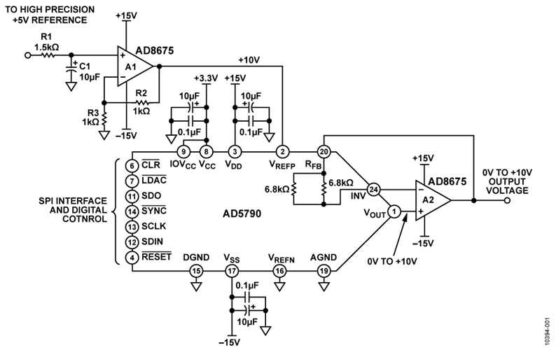
The circuit, shown in Figure 1, is a 20-bit, linear, low noise, precision, unipolar (+10 V) voltage source with a minimum amount of external components. The AD5790 DAC is a 20-bit, unbuffered voltage output DAC that operates from a bipolar supply of up to 33 V. The AD5790 accepts a positive reference input range of 5 V to VDD − 2.5 V, and a negative reference input range of VSS + 2.5 V to 0 V. Both reference inputs are buffered on the chip, and external buffers are not required. The AD5790 offers a relative accuracy specification of ±2 LSB maximum, and operation is guaranteed monotonic with a −1 to +2 LSB maximum DNL specification.
The AD8675 precision op amp has low offset voltage (75 μV maximum) and low noise (2.8 nV/√Hz typical) and is an optimum output buffer for the AD5790. The AD5790 has two internal matched 6.8 kΩ feedforward and feedback resistors, which can either be connected to the AD8675 op amp to provide a 10 V offset voltage for a ±10 V output swing, or connected in parallel to provide bias current cancellation. In this example, a unipolar +10 V output is demonstrated, and the resistors are used for bias current cancellation. The internal resistor connection is controlled by setting a bit in the AD5790 control register (see AD5790 data sheet).
The digital input to the circuit is serial and is compatible with standard SPI, QSPI, MICROWIRE®, and DSP interface standards. For high accuracy applications, the compact circuit offers high precision, as well as low noise—this is ensured by the combination of the AD5790 and AD8675 precision components.


Circuit Description
The digital-to-analog converter (DAC) shown in Figure 1 is the AD5790, a high voltage, 20-bit converter with SPI interface, offering ±2 LSB INL, −1 to +2 LSB DNL, and 8 nV/√Hz noise spectral density. The AD5790 also exhibits an extremely long term linearity error stability of 0.1 LSB.
Figure 1 shows the AD5790 in a unipolar buffered configuration. The output buffer is the AD8675, used for its low noise and low drift. This amplifier is also used (A1) to amplify the +5 V reference voltage from the low noise precision reference, in this case a Krohn Hite Model 523 precision reference. The resistors R2 and R3 in this gain circuit are precision metal foil resistors with 0.01% tolerance and a temperature coefficient of 0.6 ppm/°C. For optimum performance over temperature, R2 and R3 should be in a single package, such as the Vishay 300144 or VSR144 series. R2 and R3 are selected to be 1 kΩ to keep noise in the system low. R1 and C1 form a low-pass filter with a cutoff frequency of approximately 10 Hz. The purpose of this filter is to attenuate voltage reference noise.
Linearity Measurements
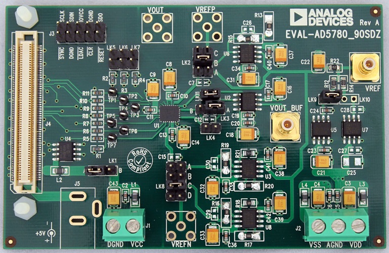
The precision performance of the circuit shown in Figure 1 is demonstrated on the EVAL-AD5790SDZ evaluation board using an Agilent 3458A multimeter. Figure 2 shows that the integral nonlinearity as a function of DAC code is well within the specification of ± 2 LSB from 0°C to 105°C.
Figure 3 shows that the differential nonlinearity as a function of DAC code is within the −1 LSB to +2 LSB specification.


Noise Drift Measurements
To be able to realize high precision, the peak-to-peak noise at the circuit output must be maintained below 1 LSB, which is 9.5 μV for 20-bit resolution and a +10 V unipolar voltage range.
A real-time noise application will not have a high-pass cutoff at 0.1 Hz to attenuate 1/f noise but will include frequencies down to dc in its pass band. With this in mind, the measured peak-to-peak noise is shown in Figure 4. In this case, the noise at the output of the circuit was measured over a period of 100 seconds, effectively including frequencies as low as 0.01 Hz in the measurement.
A temperature controlled ultralow noise reference was required for this measurement so as not to dominate the noise performance.
The zero-scale output voltage exhibits the lowest noise because it represents the noise from the DAC core only. The noise contribution from each voltage reference path is attenuated by the DAC when the zero-scale code is selected.


As the time period over which the measurement is taken is increased, lower frequencies will be included, and the peak-to-peak value will increase. At low frequencies, temperature drift and thermocouple effects become contributors to noise. These effects can be minimized by choosing components with low thermal coefficients.
Complete schematics and layout of the printed circuit board can be found in the CN-0257 Design Support package: www.analog.com/CN0257-DesignSupport.
Common Variations
The AD5790 will support a wide variety of output ranges from 0 V to +5 V up to ±10 V, and values in between. If a bipolar configuration is required, then the VREFN pin needs to be supplied with an inverted high precision reference voltage. Again, precise amplifier technology and precision temperature stable resistors are required.
The AD8676 is a dual version of the AD8675 op amp and can be used in the circuit if desired.
Circuit Evaluation & Test
Equipment Required
- System Demonstration Platform (EVAL-SDP-CB1Z)
- EVAL-AD5790SDZ evaluation board and software
- Krohn-Hite Model 523 precision reference
- Agilent 3458A multimeter
- PC (Windows 32-bit or 64-bit OS)
- National Instruments GPIB to USB-B interface cable
- SMB cable (2)
Software Installation
The AD5790 evaluation kit includes self-installing software on a CD. The software is compatible with Windows XP (SP2) and Vista (32-bit and 64-bit). If the setup file does not run automatically, you can run the setup.exe file from the CD.
Install the evaluation software before connecting the evaluation board and SDP board to the USB port of the PC to ensure that the evaluation system is correctly recognized when connected to the PC.
- After installation from the CD is complete, power up the AD5790 evaluation board as described in the Power Supplies section. Connect the SDP board (via either Connector A or Connector B) to the AD5790 evaluation board and then to the USB port of your PC using the supplied cable.
- When the evaluation system is detected, proceed through any dialog boxes that appear. This completes the installation.
Functional Diagram
A functional diagram of the test setup is shown in Figure 6.
Power Supplies
The following external supplies must be provided:
- 3.3 V between the VCC and DGND on Connector J1 for the digital supply of the AD5790. Alternatively, place Link 1 in Position A to power the digital circuitry from the USB port via the SDP board (default).
- +12 V to +16.5 V between the VDD and AGND inputs of J2 for the positive analog supply of the AD5790.
- −12 V to −16.5 V between the VSS and AGND inputs of J2 for the negative analog supply of the AD5790.
- +5 V precision reference connected to SMB connector labeled VREF.


Default Link Option Setup
The default link options are listed in Table 1. By default, the board is configured with VREFP = +10 V and VREFN = −10 V for a ±10 V output range.
| Link No. | Option |
| LK1 | A |
| LK2 | B |
| LK3 | A |
| LK4 | Removed |
| LK5 | Removed |
| LK6 | Removed |
| LK7 | Removed |
| LK8 | C |
| LK9 | Inserted |
| LK11 | Inserted |
In order to configure the board for the circuit shown in Figure 1, the following changes must be made to the default link configuration in Table 1:
- Place LK3 in position A.
- Remove LK4.
- Place LK8 in position B.
- Remove LK9.
These changes configure the output buffer amplifier for a gain of 1 and connect the VREFN pin of the AD5790 to ground. In addition, the board is now configured to accept a precision +5 V reference on the SMB connector labeled VREF.
Please refer to User Guide UG-342 for more information on the EVAL-AD5790SDZ test setup.
Test
The VOUT_BUF SMB connector is connected to the Agilent 3458A multimeter. The linearity measurements are run using the Measure DAC Output Tab on the AD5790 GUI.
The noise drift measurement is measured on the VOUT_BUF SMB connector also. The output voltage is set using the Program Voltage tab in the AD5790 GUI. The peak-to-peak noise drift is measured over 100 seconds.
For more details on the definitions and how to calculate the INL, DNL, and noise from the measured data, see the "TERMINOLOGY" section of the AD5790 data sheet and also the following reference: Data Conversion Handbook, "Testing Data Converters," Chapter 5, Analog Devices.