


Overview
Design Resources
Design & Integration File
- Schematic
- Bill of Materials
- Gerber Files
- PADS Files
- Assembly Drawing
Evaluation Hardware
Part Numbers with "Z" indicate RoHS Compliance. Boards checked are needed to evaluate this circuit.
- EVAL-CN0211-EB1Z ($105.93) IF Band-Pass Filter Bank Switching Network for Wireless Infrastructure
Features & Benefits
- RF signal routing techniques
- Selectable filter response
- Excellent off isolation of -50 dB at 200 MHz
Product Categories
Markets and Technologies
Parts Used
Documentation & Resources
-
MT-101: Decoupling Techniques2/14/2015PDF954 kB
-
CN-0211: IF Band-Pass Filter Bank Switching Network for Wireless Infrastructure6/13/2012PDF245 kB
Circuit Function & Benefits
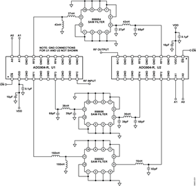
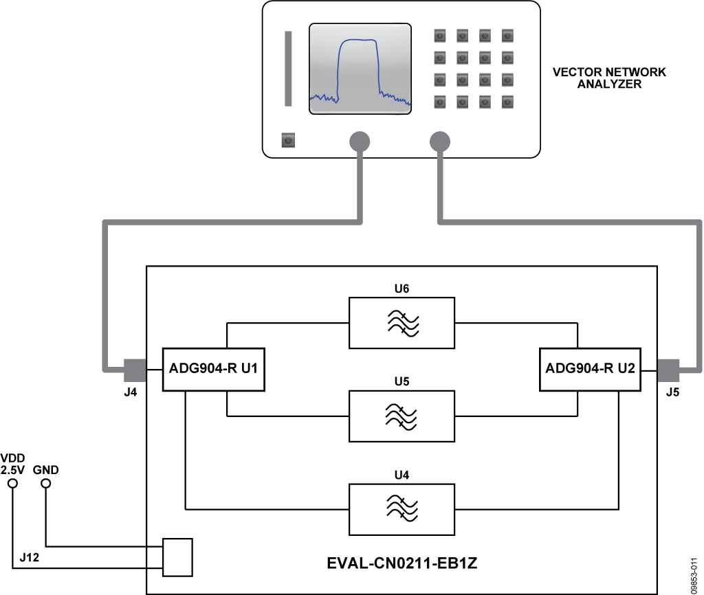
The function of the circuit, shown in Figure 1, is to route an RF signal through an IF band-pass filter bank. The circuit uses three 140 MHz IF SAW filters with different bandwidths and two ADG904-R SP4T CMOS RF switches. The ADG904-R switches control which band-pass filter the RF signal will pass through. Only one filter is selectable at a time. The typical name given to this type of switching is “filter bank switching.” This application is very common in wireless infrastructure applications, such as cell phone base stations and point-topoint radio RF front ends. Selecting IF filters with different bandwidths results in more flexibility in controlling the various data rates in these systems.
Insertion loss versus frequency in the IF band must be flat to achieve optimum system performance. The ADG904-R switch is ideally suited for this circuit because it has very flat insertion loss versus frequency. The insertion loss also remains flat over the supply voltage and temperature range. Switch off isolation is another very important parameter to maximize the performance of this circuit. The ADG904-R has excellent off isolation of greater than −50 dB up to 200 MHz.
Circuit Description
The circuit consists of two ADG904-R CMOS RF switches and three IF SAW filters connected as shown in Figure 1. The switches have a supply voltage range of 1.65 V to 2.75 V. In this evaluation, a nominal value of 2.5 V is used. The RF input is connected to Pin 10 (RFC) of the ADG904-R switch, U1. The ADG904-R switch is a SP4T switch where the RFC pin is the common connection to all four switches (RF1, RF2, RF3 and RF4). Pin 4 of U1 (RF1) is connected to the input of the Triquint 856592 SAW filter. This filter is a single ended filter with a characteristic impedance of 50 Ω. It has a center frequency of 140 MHz and a typical 1 dB bandwidth of 20.7 MHz. Note that lumped element matching is required to achieve the optimum 50 Ω termination impedance. The output of the filter is connected to pin 17 (RF2) of the ADG904-R, U2.
Similarly, the second SAW filter (Triquint 856684) is connected to U1 and U2. In this case, the filter is connected to Pin 17 (RF2) of U1 and Pin 4 (RF1) of U2. The 856684 filter has a center frequency of 140 MHz and a typical 1 dB bandwidth of 16.18 MHz.
The third SAW filter (Triquint 856656) is connected to Pin 7 (RF3) of U1 and Pin 14 (RF4) of U2. The 856656 filter has a centre frequency of 140 MHz and a typical 1 dB bandwidth of 11.82 MHz.
It is important to use the PCB land layout pattern recommended by the manufacturer of the SAW filters. To achieve the maximum isolation from the input port to the output port, a plated slot was positioned under the filter. Improving this isolation enables the full out-of-band attenuation to be achieved and minimizes the in-band ripple. Each filter is matched to 50 Ω on the input port and output port using 0603 size inductor and capacitor lumped elements. This is an important aspect for achieving good performance from the circuit evaluation board. To further improve isolation, the 50 Ω transmission lines that connect the filters to the switches and to the RF edge connectors are designed as coplanar waveguides.
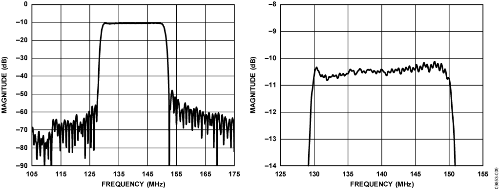
The standalone insertion loss vs. frequency for the 11.82 MHz bandwidth filter is shown in Figure 3. This data was measured with the filter on a separate circuit evaluation PCB with the same transmission line design and matching components, but with no switches in the RF path. This response is used as reference data. The insertion loss at 140 MHz was −9.17 dB, which is consistent with the data sheet value of −9.2 dB typical.

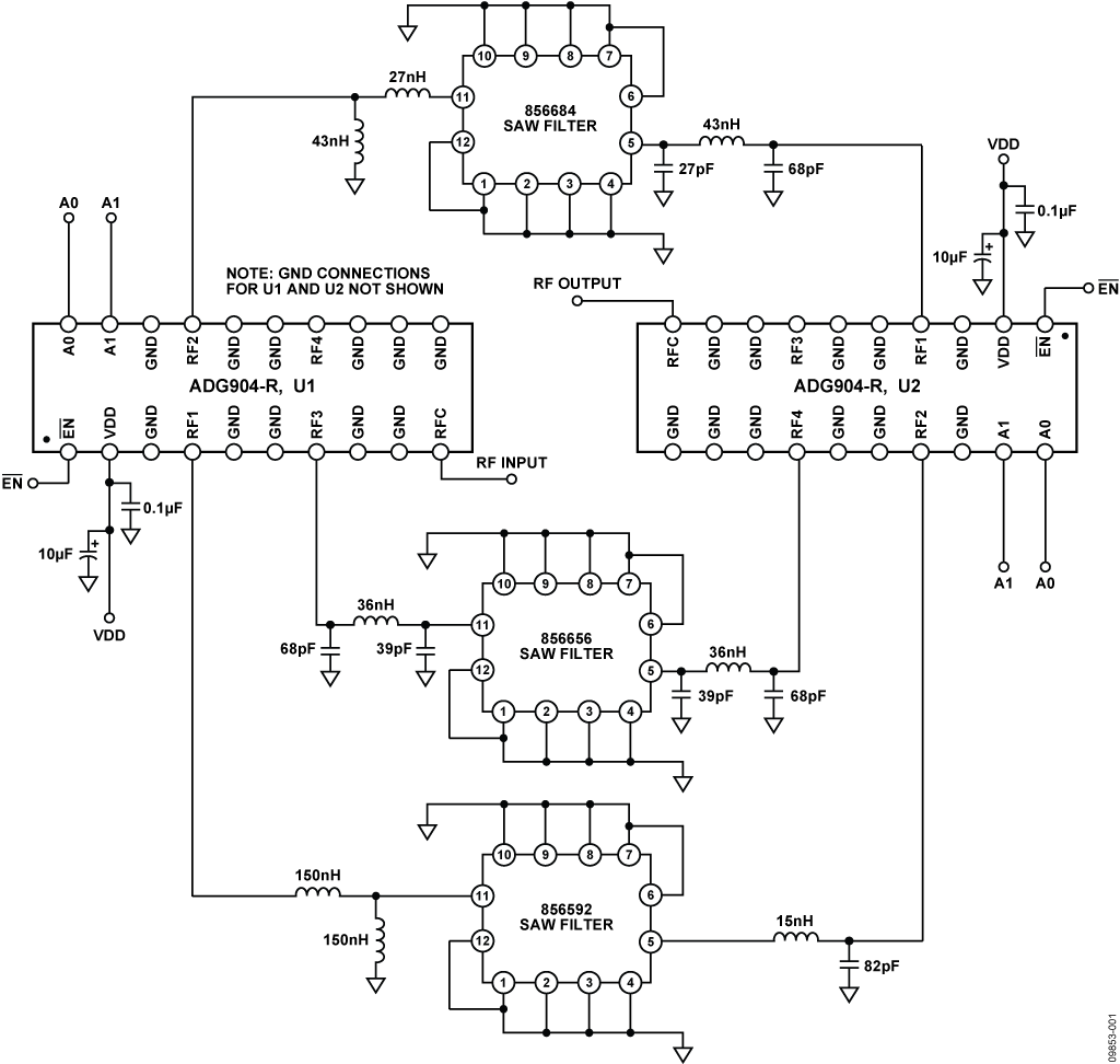

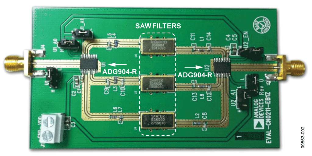
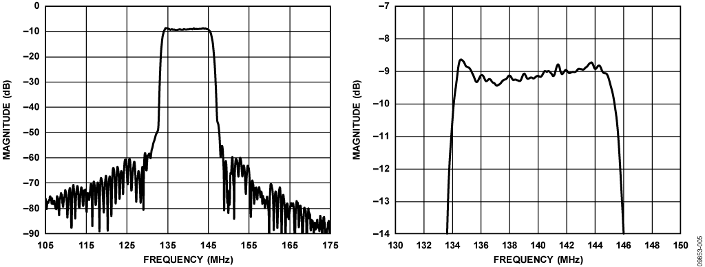
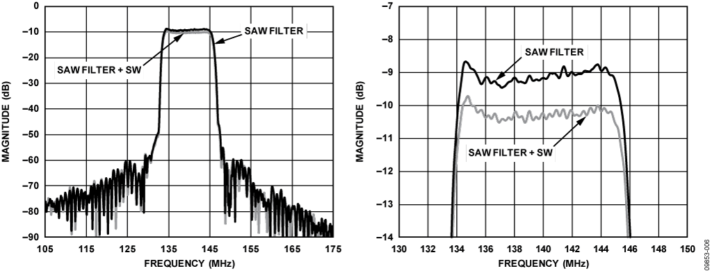
Figure 4 shows test results from the circuit evaluation PCB when the ADG904R switches are selecting the 856656 SAW filter. The response compares well to the standalone response, which is also included in the plot for reference. Due to the loss of the two ADG904-R switches in series, the insertion loss of the filter has increased by 1 dB. Ripple in the pass band is of importance in wireless infrastructure applications. The ripple across the band is 0.47 dB from the minimum to maximum peak within the pass band of 135.5 MHz to 144.5 MHz. This level is well within the data sheet specification for ripple, which is 0.8 dB max. The high off isolation of the switches is critical in this application to minimize leakage from one filter channel to the next. Poor switch off isolation would increase the in-band insertion loss and ripple of the filter. No evidence of this is visible in these test results.
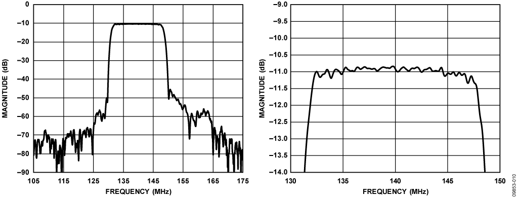
Figure 5 and Figure 6 show the 856592 and 856684 SAW filter channel test results, respectively. The results shown include the loss from the two ADG904-R switches in series. This loss is approximately 1.0 dB. Both filter channels show good flat insertion loss, plus high out-of-band attenuation levels. The results shown are within the manufacturers data sheet tolerances and clearly show that the ADG904-R switches are not introducing any ripple, mismatch, or affecting the flatness of the filters in any way.


Common Variations
The absorptive version of the ADG904 switch can also be used in this filter bank switching circuit. The absorptive version contains 50 Ω shunt resistors on the RFx ports. This results in a good 50 Ω match when the switch is in the off state. This is important in some applications where reflected signals in the off channels need to be absorbed.
The circuit can be easily scaled to include more or fewer filter channels. Depending on the number of channels, other switches from the ADG9xx family may be better to use and offer more flexibility with layout. The ADG936 is a dual SPDT switch, the ADG918 is an SPDT switch, and the ADG901 is an SPST switch. All of these switches are available in both absorptive and reflective configurations.
Circuit Evaluation & Test
The circuit is designed to be connected to a vector network analyzer (VNA) via SMA type connectors. The SMA connectors on the board are female. To switch between each filter channel there are jumper terminals on the board that can be manually changed. Note that one of the switch throws in each ADG904-R switch is not used. Therefore, when these unused switches are selected, the RF input and RF output ports are isolated, i.e., the switches are not connected to a filter.

Equipment Needed
- Vector Network Analyzer, Hewlett Packard 8753E with Hewlett Packard 85033D 3.5 mm Calibration Kit, or equivalent.
- EVAL-CN0211-EB1Z Circuit Evaluation Board
- Power supply (2.5V)
- Coaxial RF cable with 3.5 mm type connectors
Setup and Test
The test setup is shown in Figure 7. The VNA is connected to the circuit evaluation board through 3.5 mm connector type cables. Full two port calibration of the VNA to the end of the cables will be required before testing of the circuit evaluation board. Table 1 shows the logic states to enable each individual filter channel.
| Filter | EN | ADG904-R U1 |
ADG904-R U2 |
||
| A0 | A1 | A0 | A0 | ||
| U6 | 0 | 1 | 0 | 0 | 0 |
| U5 | 0 | 0 | 1 | 1 | 1 |
| U4 | 0 | 0 | 0 | 1 | 0 |