CN0181

Overview
Design Resources
Device Drivers
Software such as C code and/or FPGA code, used to communicate with component's digital interface.
AD5446 GitHub no-OS Driver Source Code
AD5541A - No-OS Driver for Renesas Microcontroller Platforms
AD5541A - No-OS Driver for Microchip Microcontroller Platforms
Features & Benefits
- True 16 bit voltage output DAC w/buffer
- Small footprint saves board space and lowers cost
- Low power consumption
Product Categories
Markets and Technologies
Parts Used
Documentation & Resources
-
The Data Conversion Handbook, 20051/2/2005
-
MT-016: Basic DAC Architectures III: Segmented DACs2/14/2015PDF79 kB
-
MT-015: Basic DAC Architectures II: Binary DACs (Rev. A)3/20/2009PDF100 kB
Circuit Function & Benefits
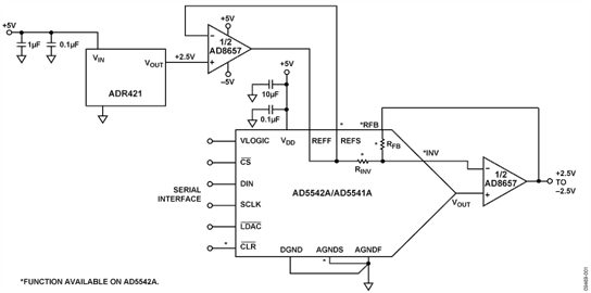
Looking for true 16-bit level set performance in a small package and ultralow power? This circuit provides a low power, small footprint solution for precision 16-bit digital-to-analog conversion using the AD5542A/AD5541A voltage output DAC with the ADR421BRZ voltage reference and the 20 μA AD8657 as the voltage reference buffer.
The reference buffer is critical to the design because the input impedance at the DAC reference input is heavily code- dependent and will lead to linearity errors if the DAC reference is not adequately buffered. With a high open-loop gain of 120 dB, the AD8657 has been proven and tested to meet the settling time, offset voltage, and low impedance drive capability required by this circuit application.
The combination of parts shown in Figure 1 minimizes PC board area, as well as power dissipation. The AD5542A is available in a 3 mm × 3 mm, 16-lead LFCSP or 16-lead TSSOP package. The AD5541A is available in 3 mm × 3 mm, 10-lead LFCSP or 10-lead MSOP.
This combination of parts provides industry-leading 16-bit integral nonlinearity (INL) of ±1 LSB and differential nonlinearity (DNL) of ±1 LSB with guaranteed monotonicity, as well as low power, small PCB area, and cost effectiveness.


Circuit Description
For a perfect DAC with no errors, output voltage is dependent on the reference voltage, as shown in the following equation:

where D is the decimal data word loaded in the DAC register, and N is the resolution of the DAC.
For a reference of 2.5 V, and N = 16, the equation simplifies to the following:

This gives a VOUT of 1.25 V at mid-scale, and 2.5 V at full-scale.
The LSB size is 2.5 V/65,536 = 38.1 μV.
One LSB at 16 bits is also 0.0015% of full-scale or 15 ppm FS.
The initial room temperature accuracy of the ADR421 (B grade) reference is 0.04%, which is approximately 27 LSBs at 16 bits. This initial error can be removed with a system calibration. The temperature coefficient of the ADR421 (B grade) is 1 ppm/°C typical, 3 ppm/°C maximum.
Assuming a perfect reference (the reference error removed by system calibration), the worst-case unipolar output voltage (including errors) for the AD5542A can be calculated from the following equation:

where:
VOUT−UNI is unipolar mode worst-case output.
D is code loaded to the DAC.
VREF is reference voltage applied to the DAC (assumed to have no errors).
VGE is gain error in volts. (Note that the offset error of the reference buffer must be included in the gain error, hence the op amp chosen for the reference buffer must have low input offset voltage.)
VZSE is zero-scale error (offset error) in volts. (Note that the offset voltage of the optional output buffer amplifier would add to this error.)
INL is integral nonlinearity of the DAC in volts. (Note that the nonlinearity of the optional output buffer amplifier would add to this error.)
This circuit utilizes the AD5542A voltage output DAC, providing true 16-bit INL and DNL. The DAC architecture of the AD5541A/AD5542A is a segmented R-2R voltage mode DAC. With this type of configuration, the output impedance is independent of code, but the input impedance seen by the reference is heavily code dependent. For this reason, the reference buffer choice is very important to account for code-dependent reference current, which may lead to linearity errors if the DAC reference is not adequately buffered. The op amp open-loop gain, offset voltage, offset error temperature coefficient, and voltage noise are also important selection criteria when selecting a reference buffer with precision voltage output DACs. Offset errors in the reference circuit result in gain error on the DAC output.
This circuit employs a low power AD8657 CMOS op amp in a force and sense configuration (Kelvin sensing) as the low impedance output reference buffer for the AD5542A. The AD8657 has an open-loop gain of 120 dB and is a precision, 18 V, 50 nV/√Hz op amp. With a maximum offset voltage of 350 μV, typical drift of less than 2 μV/°C, and noise of 5 μV p-p (0.1 Hz to 10 Hz), the AD8657 is well suited for applications where error sources need to be minimized. The other half of the AD8657 is used as the output amplifier.
The AD5542A can be operated in either buffered or unbuffered mode. The application and its requirements on settling time, load impedance, noise, etc., determine which mode of operation to be used. The output buffer can be chosen to optimize dc precision or fast settling time. Output impedance of the DAC is constant (typically 6.25 kΩ) and code-independent, but to minimize gain errors, the input impedance of the output amplifier should be as high as possible. The output amplifier should also have a 3 dB bandwidth of 1 MHz or greater. The output amplifier adds another time constant to the system, hence increasing the settling time of the output. A wider bandwidth op amp results in a shorter effective settling time of the combined DAC and amplifier.
The combination of parts shown in Figure 1 minimizes PC board area. The AD5542A is available in a 3 mm × 3 mm, 16-lead LFCSP or 16-lead TSSOP package. The AD5541A is available in 3 mm × 3 mm, 10-lead LFCSP or 10-lead MSOP.
Note that the AD5541A does not contain the Kelvin sense lines on the reference and the ground, the Clear function, or the RFB and RINV resistors.
The AD8657 and ADR421 are available in an 8-lead MSOP.
Measured results show that the AD5542A/AD5541A is an excellent candidate for high accuracy, low noise performance level setting applications. The level of dc performance is maintained using the ADR421 reference and the AD8657 as a reference buffer in this high accuracy, high performance, low power system. The measurements were made directly at VOUT without the optional output buffer connected.
Supply Current Measurements
The total supply current measurements, as well as individual component supply measurements, were taken using a precision ammeter.
The total supply current for the circuit was measured to be 0.97 mA, while the maximum data sheet specification is less than 1.5 mA.


Table 1 shows the measured results and the datasheet values. The total system solution is low in power (less than 5 mW) but high in precision.
| Data Sheet Spec (mA) | Measured (mA) | |
| ADR421BRZ, IDD1 | 0.39 (typ), 0.50 (max) | 0.316 |
| AD5542A, IDD2 | 0.3 (typ), 1.21 (max) | 0.472 |
| AD8657, IDD3 | 0.018 (typ), 0.022 (max) | 0.192 |
| IDD TOTAL | 0.708 (typ), 1.732 (max) | 0.970 |
Integral Nonlinearity and Differential Nonlinearity Measurements
INL error is the deviation in LSB of the actual DAC transfer function from an idealized transfer function. DNL error is the difference between an actual step size and the ideal value of 1 LSB. The circuit provides 16-bit resolution with ±1 LSB DNL and INL. Figure 3 and Figure 4 show the measured DNL and INL, respectively.


Layout Considerations
In any circuit where accuracy is important, it is important to consider the power supply and ground return layout on the board. The printed circuit board (PCB) containing the circuit should have separate analog and digital sections. If the circuit is used in a system where other devices require an AGND-to-DGND connection, the connection should be made at one point only. This ground point should be as close as possible to the AD5542A/AD5541A. The circuit should be constructed on a multilayer PCB with a large area ground plane layer and a power plane layer. See the MT-031 Tutorial for more discussion on layout and grounding.
The power supply to the AD5542A/AD5541A should be bypassed with 10 μF and 0.1 μF capacitors. The capacitors should be as physically close as possible to the device, with the 0.1 μF capacitor ideally right up against the device. The 10 μF capacitor should be either the tantalum bead type or ceramic type. It is important that the 0.1 μF capacitor have low effective series resistance (ESR) and low effective series inductance (ESL), such as is typical of common ceramic types of capacitors. This 0.1 μF capacitor provides a low impedance path to ground for high frequencies caused by transient currents due to internal logic switching. See the MT-101 Tutorial for more details on proper decoupling techniques.
The power supply line should have as large a trace as possible to provide a low impedance path and reduce glitch effects on the supply line. Clocks and other fast switching digital signals should be shielded from other parts of the board by digital ground.
Common Variations
For applications requiring more precision, the AD8675 op amp should be considered. It requires approximately 2.3 mA supply current at 10 V. The AD8628 zero-drift op amp is another excellent choice for use as the reference buffer in this circuit. It provides a low offset voltage and ultralow bias current with an open-loop gain of 125 dB. It requires approximately 1 mA supply current. The ADR421 (2.5 V) can be replaced by either the ADR423 (3.00 V) or ADR424 (4.096 V), which are low noise references available from the same reference family as the ADR421. The ADR441 and ADR431 ultralow noise references are also suitable substitutes, which provide 2.5 V. The AD8661 is another good choice for the optional output buffer. This is a CMOS op amp that uses the ADI patented DigiTrim® technique to achieve low offset voltage. It features low input bias current and wide signal bandwidth. It requires approximately 1 mA supply current. The AD8605 or AD8655 (both are single supply, +2.7 V to +5.5 V) would also be options, but their outputs will have nonlinearity near zero volts output because of the output stage limitations of all rail-to-rail op amps (see the MT-035 Tutorial). The AD5542A contains internal resistors (RFB and RINV), which can be used with an external op amp to provide a bipolar voltage output. (See the AD5542A data sheet for further details).