Overview
Design Resources
Design & Integration File
- Schematic
- Bill of Materials
- Gerber Files
- PAD Files
- Assembly Drawing
Evaluation Hardware
Part Numbers with "Z" indicate RoHS Compliance. Boards checked are needed to evaluate this circuit.
- EVAL-CFTL-6V-PWRZ ($23.01) Wall Power Supply for Eval Board
- EVAL-CN0150A-SDPZ ($81.21) Software Calibrated, 1 MHz to 8 GHz, 70 dB RF Power Measurement System Using the AD8318 Logarithmic Detector
- EVAL-SDP-CB1Z ($134.00) Eval Control Board SDP
Device Drivers
Software such as C code and/or FPGA code, used to communicate with component's digital interface.
Features & Benefits
- Software calibrated RF power measurement system
- RMS, peak, and crest factor outputs
- Functions from 1 MHz to 8 GHz
Product Categories
Markets and Technologies
Parts Used
Documentation & Resources
-
CN0150 Software User Guide10/18/2018WIKI
-
High Frequency Log Amps2/14/2015PDF144 kB
-
MT-101: Decoupling Techniques2/14/2015PDF954 kB
-
MT-031: Grounding Data Converters and Solving the Mystery of "AGND" and "DGND"3/20/2009PDF144 kB
-
Index10/21/2010PDF
-
Chapter I: Wireless Systems Overview10/21/2010PDF
-
Chapter II: RF/IF Components and Specifications for Receivers10/21/2010PDF
-
Chapter III: RF/IF Components and Specifications for Transmitters10/21/2010PDF
-
Chapter IV: RF Components Active and Passive Mixers10/21/2010PDF
-
Chapter V: Phase Locked Loops for High Frequency Transmitters and Receivers10/21/2010PDF
-
Chapter VI: A Detailed Look at Wireless Signal Chain Architectures10/21/2010PDF
-
Chapter VII: Receiver Optimization Using Error Vector Magnitude Analysis10/21/2010PDF
-
Chapter VIII: Design and Operation of Automatic Gain Control Loops for Receivers10/21/2010PDF
-
Chapter IX: Using Calibration and Temperature Compensation to Improve RF Power10/21/2010PDF
-
Chapter X: Measuring VSWR and Gain in Wireless Systems10/21/2010PDF
-
Chapter XI: A 2.4-GHz Direct Conversion Transmitter for WiMAX and WiBro App10/21/2010PDF
-
Chapter XII: Use a Wideband, Integer-N, PLL Synthesizer as a Direct 6-GHz Local10/21/2010PDF
-
Chapter XIII: Short Range Wireless Devices - Building a Global License-Free Sys10/21/2010PDF
-
Download All Chapters10/21/2010ZIP
Circuit Function & Benefits
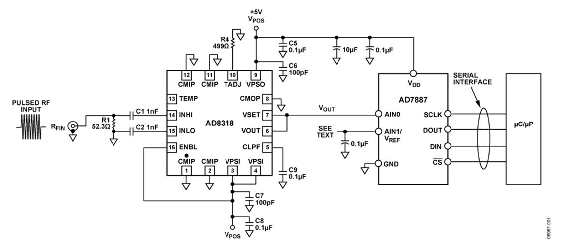
This circuit measures RF power at any frequency from 1 MHz to 8 GHz over a range of approximately 60 dB. The measurement result is provided as a digital code at the output of a 12-bit ADC with serial interface and integrated reference. The output of the RF detector has a glueless interface to the ADC and uses most of the ADC’s input range without further adjustment. A simple two-point system calibration is performed in the digital domain.
The AD8318 maintains accurate log conformance for signals of 1 MHz to 6 GHz and provides useful operation to 8 GHz. The device provides a typical output voltage temperature stability of ±0.5 dB.
The AD7887 ADC can be configured for either dual or single channel operation via the on-chip control register. There is a default single-channel mode that allows the AD7887 to be operated as a read-only ADC, thereby simplifying the control logic.
Typical data is shown for the two devices operating over a −40°C to +85°C temperature range.

Circuit Description
The RF signal being measured is applied to the AD8318. The device is configured in its so-called measurement mode, with the VSET and VOUT pins connected together. In this mode, the output voltage vs. the input signal level is linear-in-dB (nominally −24 mV/dB) and has a typical output voltage range of 0.5 V to 2.1 V.
The AD8318 output is connected directly to the AD7887, 12-bit ADC. The ADC uses its internal reference and is configured for a 0 V to 2.5 V input, resulting in an LSB size of 610 μV. With the RF detector providing a nominal −24 mV/dB, the digital resolu-tion is 39.3 LSBs/dB. With this much resolution, there is little value in trying to scale the 0.5 V to 2.1 V signal from the RF detector to exactly fit the 0 V to 2.5 V range of the ADC.
The transfer function of the detector can be approximated by the equation

where SLOPE is in mV/dB (−24 mV/dB nominal); INTERCEPT is the x-axis intercept with a unit of dBm (20 dBm nominal); and PIN is the input power expressed in dBm. A typical plot of detector output voltage vs. input power is shown in Figure 2.

At the output of the ADC, the equation can be written as

where SLOPE_ADC is in codes/dB and PIN and INTERCEPT are in dBm. Figure 3 shows a typical detector power sweep in terms of input power and observed ADC codes.
Because the slope and intercept of the system vary from device to device, a system level calibration is required. A calibration is performed by applying two known signal levels close to the endpoints of the AD8318 linear input range and measuring the corresponding output codes from the ADC. The calibration points chosen should be well within the linear operating range of the device (−10 dBm and −50 dBm in this case).
Using the two known input power levels, PIN_1 and PIN_2, and the corresponding observed ADC codes, CODE_1 and CODE_2, SLOPE_ADC, and INTERCEPT can be calculated using the following equations:

Once SLOPE_ADC and INTERCEPT are calculated and stored (in nonvolatile RAM) during factory calibration, they can be used to calculate an unknown input power level, PIN, when the equipment is in operation in the field using the equation

Figure 3 through Figure 8 show how the system transfer function deviates from this straight line equation, particularly at the endpoints of the transfer function. This deviation is expressed in dB using the equation

where CODE_OUT is the ADC output code; SLOPE_ADC is the stored ADC slope in codes/dB; INTERCEPT is the stored intercept; and PIN_TRUE is the exact (and unknown) input level.
The plots shown in Figure 3 through Figure 8 show the typical system performance that can be obtained using the AD8318 and AD7887BR in an RF power measurement system. The graphs depict the RF input power in dBm vs. the ADC output code and output error in dB (scaled on the axes on the right side of the plots). They were generated from data taken with various input power levels, frequencies, and temperatures and with both internal and external ADC voltage references. The charts show improved system performance and lower temperature drift with the use of a low drift external ADC voltage reference. (See the Common Variations section for more details about the use of an external reference.
A complete design support package for this circuit note can be found at www.analog.com/CN0150-DesignSupport.


Common Variations
The AD7887 is a 2-channel, 12-bit ADC with an SPI interface. The second input channel of this device can be connected to the AD8318 TEMP pin. This provides a convenient measure of the ambient temperature around the AD8318. Like the AD8318 power measurement output, the TEMP voltage output should also be calibrated.
If the end application requires only a single channel, the 12-bit AD7495 can be used. In multichannel applications that require multiple ADCs and DAC channels, the AD7294 can be used. In addition to providing four 12-bit DAC outputs, this subsystem chip includes four uncommitted ADC channels, two high-side current sense inputs, and three temperature sensors. Current and temperature measurements are digitally converted and available to read over the I2C-compatible interface.
The temperature stability of the circuit can be improved using an external ADC reference. The AD7887 internal 2.5 V reference has a 50 ppm/°C drift, which is approximately 15 mV over a 125°C range. Because the detector has a slope of −24 mV/dB, the ADC reference drift contributes approximately ±0.3 dB to the temperature drift error budget. The AD8318 temperature drift is approximately ±0.5 dB over a similar temperature range. (This varies with frequency. See the AD8318 data sheet for more details.)
If an external voltage reference is to be used, the ADR421 2.5 V reference is recommended. Its 1 ppm/°C temperature drift results in a reference voltage variation of only 312 µV from −40°C to +85°C. This has a negligible effect on the overall temperature stability of the system.
If a less dynamic range is required, the AD8317 (55 dB) or AD8319 (45 dB) log detector can be used. If a true rms responding power measurement is required, the AD8363 (50 dB) or ADL5902 (65 dB) can be used.
Circuit Evaluation & Test
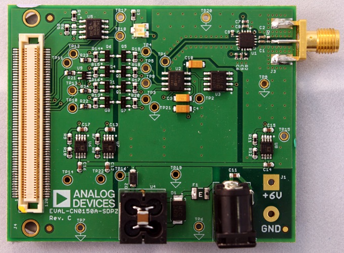
This circuit uses the EVAL-CN0150A-SDPZ circuit board and the EVAL-SDP-CB1Z System Demonstration Platform (SDP) evaluation board. The two boards have 120-pin mating connectors, allowing for the quick setup and evaluation of the circuit’s performance. The EVAL-CN0150A-SDPZ board contains the circuit to be evaluated, as described in this note, and the SDP evaluation board is used with the CN0150A evaluation software to capture the data from the EVAL-CN0150A-SDPZ circuit board.
Equipment Needed
- PC with a USB port and Windows® XP or Windows Vista® (32-bit), or Windows® 7 (32-bit)
- EVAL-CN0150A-SDPZ Circuit Evaluation Board
- EVAL-SDP-CB1Z SDP Evaluation Board
- CN0150A Evaluation Software
- Power supply: +6 V, or +6 V “wall wart”
- Environmental chamber
- RF signal source
- Coaxial RF cable with SMA connectors
Getting Started
Load the evaluation software by placing the CN0150A Evaluation Software disc in the CD drive of the PC. Using "My Computer," locate the drive that contains the evaluation software disc and open the Readme file. Follow the instructions contained in the Readme file for installing and using the evaluation software.
Functional Block Diagram
See Figure 1 of this circuit note for the circuit block diagram and the file “EVAL-CN150A-SDPZ-SCH-Rev0.pdf” for the circuit schematics. This file is contained in the CN0150 Design Support Package.
Setup
Connect the 120-pin connector on the EVAL-CN0150A-SDPZ circuit board to the connector marked “CON A” on the EVAL-SDP-CB1Z evaluation (SDP) board. Nylon hardware should be used to firmly secure the two boards, using the holes provided at the ends of the 120-pin connectors. Using an appropriate RF cable, connect the RF signal source to the EVAL-CN150A-SDPZ board via the SMA RF input connector. With power to the supply off, connect a +6 V power supply to the pins marked “+6V” and “GND” on the board. If available, a +6 V "wall wart" can be connected to the barrel connector on the board and used in place of the +6 V power supply. Connect the USB cable supplied with the SDP board to the USB port on the PC. Note: Do not connect the USB cable to the mini USB connector on the SDP board at this time.
Test
Apply power to the +6 V supply (or “wall wart”) connected to EVAL-CN150A-SDPZ circuit board. Launch the evaluation software, and connect the USB cable from the PC to the USB mini connector on the SDP board.
Once USB communications are established, the SDP board can now be used to send, receive, and capture serial data from the EVAL-CN150A-SDPZ board.
Temperature testing was performed using a Test Equity Model 107 environmental chamber. The EVAL-CN150A-SDPZ evaluation board was placed in the chamber via a slot in the test chamber door, with the SDP evaluation board extending outside.
Information and details regarding how to use the evaluation software for data capture can be found in the CN0150A evaluation software Readme file.
Information regarding the SDP board can be found in the SDP User Guide.


