ADL8130

RECOMMENDED FOR NEW DESIGNS

GaAs, pHEMT, MMIC, 0.01GHz to 8GHz, Low Noise Amplifier

Viewing:

Overview

  • High gain: 25.5dB typical from 0.01GHz to 2GHz
  • Low noise figure: <0.6dB typical from 0.5GHz to 2GHz
  • Power-down voltage pin (VPD) for enabling and disabling the amplifier
  • Single-supply bias
  • Extended operating temperature range: −55°C to +125°C
  • RoHS-compliant, 2mm × 2mm, 8-lead LFCSP
ADL8130
GaAs, pHEMT, MMIC, 0.01GHz to 8GHz, Low Noise Amplifier
ADL8130 Functional Block Diagram ADL8130 Pin Configuration
Add to myAnalog

Add product to the Products section of myAnalog (to receive notifications), to an existing project or to a new project.

Create New Project
Ask a Question

Documentation

Learn More
Add to myAnalog

Add media to the Resources section of myAnalog, to an existing project or to a new project.

Create New Project

Software Resources

Can't find the software or driver you need?

Request a Driver/Software

Tools & Simulations


Evaluation Kits

eval board
EVAL-ADL8130

Evaluating the ADL8130 GaAs, pHEMT, MMIC, 0.01GHz to 8GHz, Low Noise Amplifier

Features and Benefits

  • 4-layer, Rogers 4003C evaluation board
  • End launch, 2.9mm RF connectors
  • Through calibration path (depopulated connectors)

Product Details

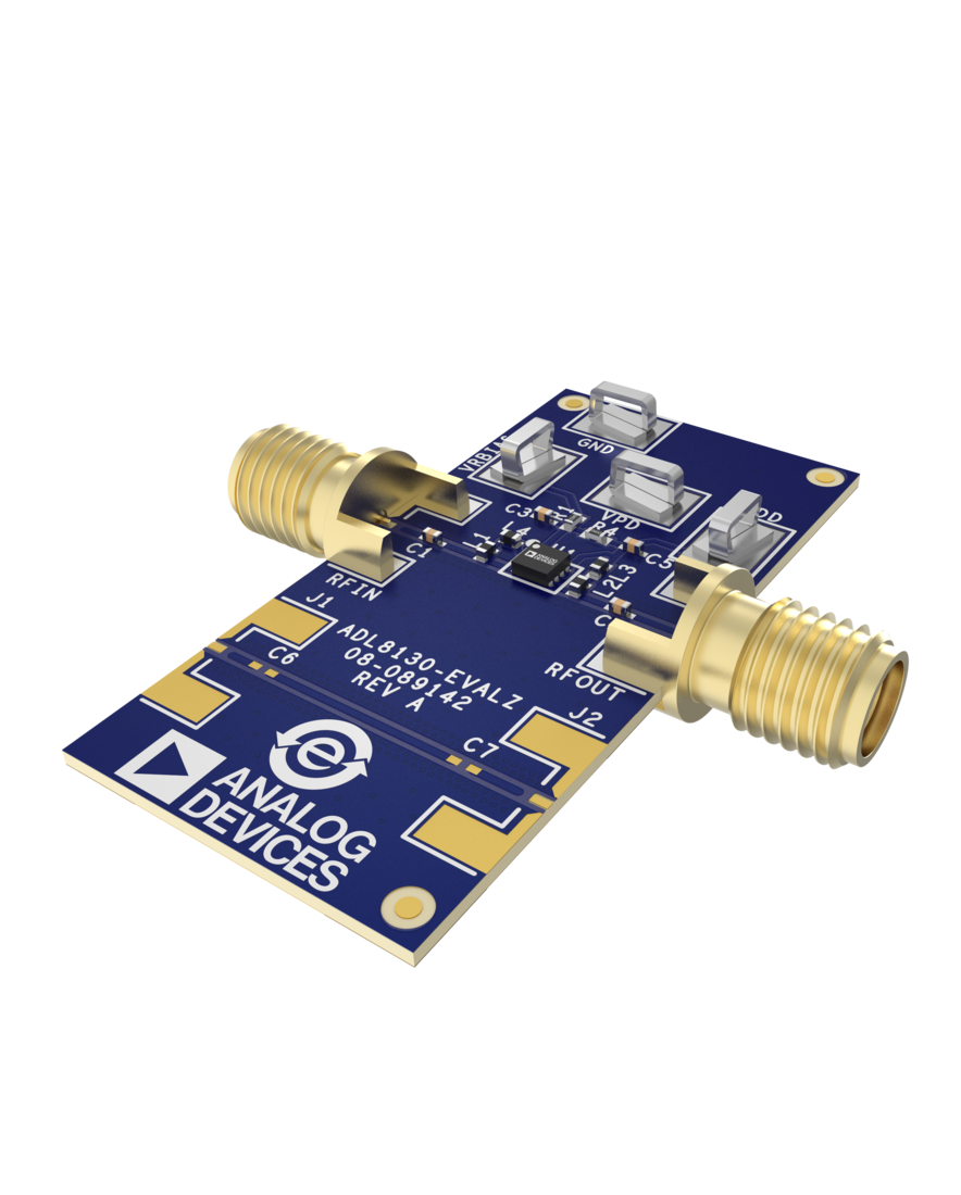
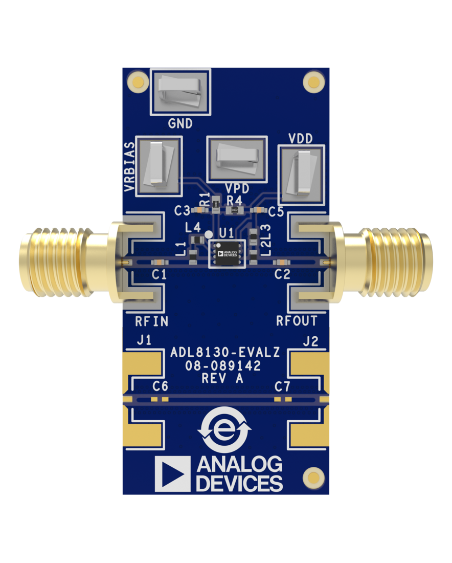
The ADL8130-EVALZ is a 4-layer printed circuit board (PCB) fabricated from 0.254mm (10mil) thick, Rogers 4003C, copper clad, forming a nominal thickness of 1.58mm (62mils). The ADL8130- EVALZ is designed to operate from 0.01GHz to 8GHz. The RFIN and RFOUT ports on the ADL8130-EVALZ are populated with 2.9mm, female coaxial connectors. The ADL8130-EVALZ is populated with components suitable for use over the entire −55°C to +125°C operating temperature range.

To calibrate out board trace losses, a through calibration path is provided between the J1 and J2 connectors. J1 and J2 must be populated with RF connectors to use the through calibration path. Refer to Figure 5 and Table 1 in user guide for the through calibration path performance for the ADL8130-EVALZ.

Access the ADL8130-EVALZ ground and drain voltage through the surface-mount technology (SMT) test point connectors, GND and VDD. A supplementary test point for VRBIAS is included for simple access on the RBIAS pin (see Figure 6 and Figure 7 in user guide for the test point locations).

The RF traces on the ADL8130-EVALZ are 50Ω, grounded, coplanar waveguide. The package ground leads and the exposed pad connect directly to the ground plane. Multiple vias connect the top and bottom ground planes with particular focus on the area directly beneath the ground paddle to provide adequate electrical conduction and thermal conduction.

The power supply decoupling capacitors on the ADL8130-EVALZ represent the configuration used to characterize and qualify the device.

For full details on the ADL8130, see the ADL8130 data sheet, which must be consulted in conjunction with this user guide when using the ADL8130-EVALZ.

EVAL-ADL8130
Evaluating the ADL8130 GaAs, pHEMT, MMIC, 0.01GHz to 8GHz, Low Noise Amplifier
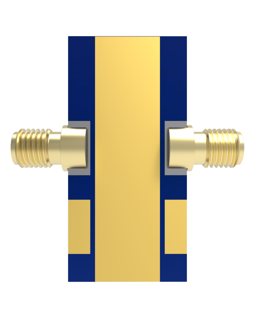
ADL8130-EVALZ Top Angle Evaluation Board ADL8130-EVALZ Top Evaluation Board ADL8130-EVALZ Bottom Evaluation Board

Latest Discussions

No discussions on ADL8130 yet. Have something to say?

Start a Discussion on EngineerZone®

Recently Viewed